0
\$\begingroup\$

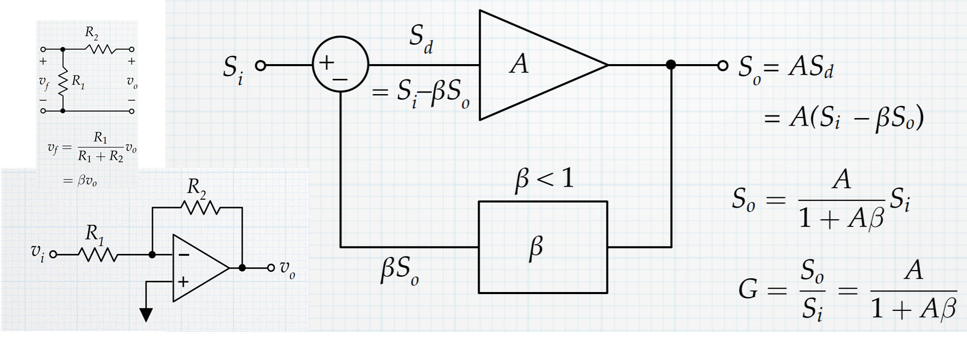
enter image description here

Hi,

I'm studying op amp and it feedback to control the gain. I do not understand how we can go from looking at the circuit of the op amp and determine the beta values. How did the term B (beta) equal to the voltage divider (R1/R2+R1)? Sf or Vf, how did they redraw the op amp circuit or the feedback block diagram into an voltage divider??

\$\endgroup\$

3 Answers 3

1
\$\begingroup\$

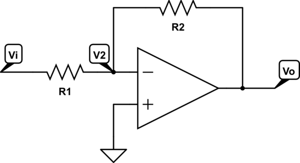
Consider the schematic. Assume that the op-amp is ideal and hence no current flows to the inputs.

schematic

simulate this circuit – Schematic created using CircuitLab

The feedback voltage Vf is the voltage at the input, at node V2, because of the output voltage Vo.

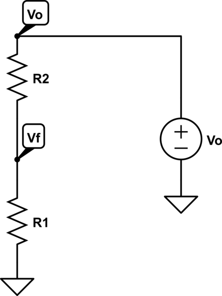
To get this, let's switch of the source at node Vi and connect a source at Vo.

schematic

simulate this circuit

That's how the voltage divider comes in feedback path.

\$\endgroup\$
4
  • \$\begingroup\$ Why do we have to turn off the source voltage when analyse Vf? What if we want Vd/Vs? \$\endgroup\$
    – Ace8888
    Commented Oct 29, 2017 at 3:50
  • \$\begingroup\$ @Ace8888 I want the \$\beta\$, the fraction of output feedback to input. But V2 will have effect from Vi and Vo .. I want to get the effect from Vo only. That’s why I switched off Vi... what is Vd and Vs? \$\endgroup\$
    – nidhin
    Commented Oct 29, 2017 at 3:55
  • \$\begingroup\$ Vd is the voltage difference from V+ & V- and Vs is the source Vi \$\endgroup\$
    – Ace8888
    Commented Oct 29, 2017 at 4:02
  • \$\begingroup\$ @Ace8888 you switch off Vo and and connect a source at Vs. That will give you the contribution of Only Vs at the op-amp terminals.. which will also be a voltage divider in this case.. \$\endgroup\$
    – nidhin
    Commented Oct 29, 2017 at 4:09
1
\$\begingroup\$

Electric circuits have totally different structure than block diagrams. In electric circuits there are voltages between the nodes and those voltages cause currents along the wires and components between the nodes. In addition there are multiport parts like amplifiers or transformers.

In block diagrams there are no such things. They are graphical presentations how quantities depend on each other. Block diagram is one way to write a group of equations.

There's no look-alike equivalence between circuit diagrams and block diagrams because the blocks present terms in equations, not components. Thus it's totally useless to try to find the little step that transforms the opamp circuit to your generic feedback block diagram, altough the resistors a little resemble rectangular blocks.

We have several ways to write the circuit equations for a circuit. They all lead to the same solution of currents and voltages, but as block diagrams they are totally different. Some of them can resemble your generic feedback model.

Lets try one of the possiblities. The output voltage U2 is negated and amplified opamp input voltage Ux. We write it U2 = -A*Ux

The opamp input voltage Ux is a superposition of U1 and U2. From both sources the Ux is given through a voltage divider. This assumes the opamp input current to be zero, there's the same current I through R1 and R2.
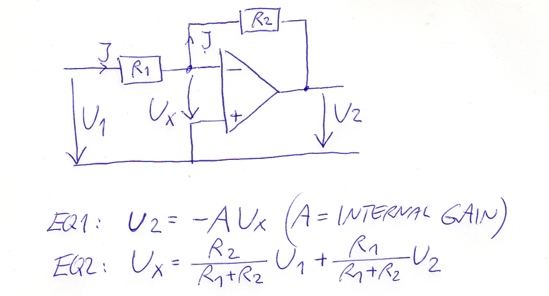
enter image description here

This is far away from the generic feedback model equations. We must write equivalent equations with non-physical quantities which we form by multiplying the equations retaining the equality:
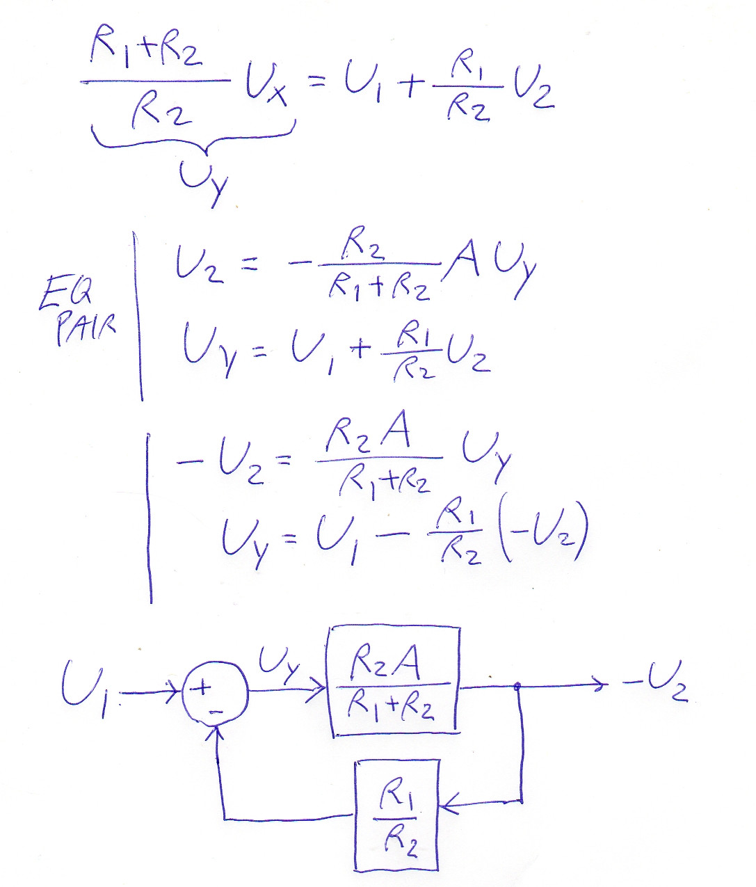
enter image description here

U1 is made separate term by multiplying EQ2 by (R1+R2)/R2. In the place of Ux we have non-physical quantity Uy. It's compensated in EQ1 by dividing. In the place of U2 we have its negation -U2.

Now the system is formally like the generic feedback diagram. From it we for example see directly: When we let the gain A to grow to infinity, the circuit amplifies the usual way: U2 = -(R2/R1)*U1. That's the inverse of the feedback factor.

\$\endgroup\$
2
  • \$\begingroup\$ +1 for 'we're dealing with different things', and it's the equations that matter, not the components \$\endgroup\$
    – Neil_UK
    Commented Oct 29, 2017 at 5:29
  • \$\begingroup\$ @Ace8888 I edited the answer to obey the form of your generic feedback diagram. \$\endgroup\$
    – user136077
    Commented Oct 29, 2017 at 13:26
0
\$\begingroup\$

The given expression for the gain G is correct for the block diagram - however, it does NOT apply to the shown opamp circuit with resistive feedback (R1-R2).

The general formula for feeedback loop is:

H(s)=-Hf * A/(1+Hr * A)

with Hf: Forward (reduction) factor; Hr=Return factor (feedback factor beta).

For the shown circuit: Hf=R2/(R1+R2) and Hr=(beta)=R1/(R1+R2).

For a very large value of A (we set it to infinity) this results in H=-R2/R1.

Definitions:

Hf=part of input voltage arriving at the opamp input (setting Vout=0) and Hr=part of the output voltage arriving at the opamp input (setting Vin=0).

\$\endgroup\$

Your Answer

By clicking “Post Your Answer”, you agree to our terms of service and acknowledge you have read our privacy policy.

Not the answer you're looking for? Browse other questions tagged or ask your own question.