2
\$\begingroup\$

I've seen a number of posts out there concerning adding/removing DC biases, and I can't seem to find one that has been directly applicable to my problem.

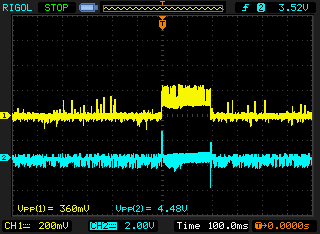
Question: How do I remove the 1.5V DC step that occurs when the MCP4921 outputs audio?

Problem: When I play sound, there is a clicking noise that occurs at the start and end of the audio sample. I am sure that I have removed any transients in my original samples by adding fade in/fade out, and the hex files that I have generated from these samples do not contain any transients at the beginning or end, either, as they begin and end with 0x00's. Other background information, such as my audio driver code, can be found here: Audio Noise: ATMEGA328P, MCP4921, and LM386

I have tried the following two possible solutions from different posts, with no change in the output characteristic:

  • Adding a 1.5V DC Bias to the MCP4921 output, using the topology of the first answer from this post: DC biasing audio signal
  • Adding two diodes between the output (after the AC coupling cap) and 5V power supply, to get an equivalent diode voltage drop to the step I am seeing

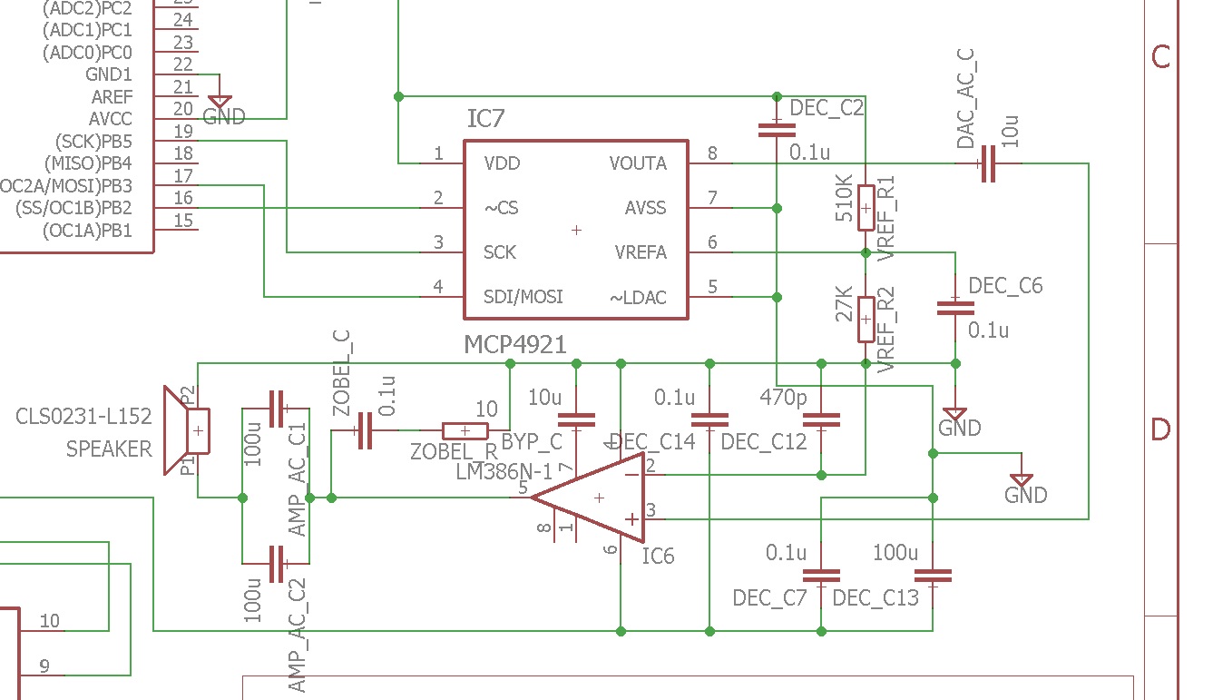
See attached for screenshot of the oscilloscope, with the probe being on the MCP4921 output (after the AC coupling cap). Also attached is the schematic. The schematic does not show the two possible solutions which I mentioned above. The purpose of the V_REF Resistors is to make a voltage divider that will give 0.25V at the V_Ref of the MCP4921. This was done so that the default gain of the amplifier, 20, will produce a 5Vp-p signal at the speaker.

Oscilloscope Output, Yellow is output of the MCP4921, past the AC Coupling cap, and Blue is at the speaker

EAGLE Schematic for Audio Module

Thank You,

\$\endgroup\$
3
  • 1
    \$\begingroup\$ Just curious, what's the purpose of DEC_C12 on the negative input of the LM386N? The negative input is already shorted to ground, so the cap seems to be useless \$\endgroup\$ Commented Nov 13, 2017 at 3:43
  • \$\begingroup\$ I built my audio circuit according to this link: circuitbasics.com/…. There, the person says that the 470pF cap is to filter any noise from radio interference on the audio input line. Now that I am thinking about it, would my circuit need this since I'm getting input straight from a DAC instead? Also, I noticed he might have made a mistake, since he said between ground and the positive input, but in his schematic its between ground and the negative input, so it would be shorted, like you are indicating? \$\endgroup\$ Commented Nov 13, 2017 at 16:05
  • \$\begingroup\$ Yes, if your audio source (DAC) is so close and your traces are nice and short I'd think you'd be able to omit it. But just in case, I'd add it on your PCB and make it a do not place (DNP) in case you'd want to add one later. And yes, the schematic is wrong -- the cap should be connected to the positive input pin to ground. \$\endgroup\$ Commented Nov 13, 2017 at 19:02

2 Answers 2

1
\$\begingroup\$

You need to change your software so that between outputs of the audio you set the DAC to the mean voltage of the audio - presumably half-scale (0x80).

Then the audio will not be on a pedestal.

Most of these types of DACs use unsigned binary coding. To use it for audio you need to offer the audio by half-full scale so that you can go either positive or negative relative to the zero level.

Between audio clips you need to set your DAC to hat same level.

It doesn't look like you need any hardware changes.

\$\endgroup\$
2
  • \$\begingroup\$ I tried your solution, by just doing an if...else statement, where if a certain amount of time elapsed, a sound would play, else I am just constantly inputting 0x80 to the DAC like you suggested. Although the zero of the "off" waveform is now in line with the "on" waveform, I still get the clicks in the beginning and end when the sound plays. \$\endgroup\$ Commented Nov 13, 2017 at 21:38
  • \$\begingroup\$ You also need to ensure that the clips start and end with 0x80 to avoid a transient. You may also need to fade-in and out. \$\endgroup\$ Commented Nov 14, 2017 at 0:29
0
\$\begingroup\$

In addition to Kevin's fix, I would suggest you generate a full scale triangle waveform to verify your DAC output is monotonic and symmetrical to Vdd then the LM386 pin 3(+in) needs to be biased to Vdd/2 so you can bypass the 10uF ac coupling for DC coupling. Then the (-) should have the same value R to reduce (Iin bias * R)*Av = Vout offset error.

\$\endgroup\$
2
  • \$\begingroup\$ When you say monotonic and symmetrical to Vdd, do you mean that the triangle wave should start at 0 V and peak at Vdd, and then go back down to 0 V? Assuming this is what you meant, I don't reach Vdd in my circuit because my Vref is 0.25 V on the DAC, so the waveform goes between 0 and 0.25 V? \$\endgroup\$ Commented Nov 13, 2017 at 21:30
  • \$\begingroup\$ Whatever, try a full scale triangle and verify signal integrity. Right now it has many issues \$\endgroup\$
    – D.A.S.
    Commented Nov 14, 2017 at 4:08

Your Answer

By clicking “Post Your Answer”, you agree to our terms of service and acknowledge you have read our privacy policy.

Not the answer you're looking for? Browse other questions tagged or ask your own question.