The Mazzilli Zero Voltage Switching (ZVS) driver consists of two parts:
- The switching circuit
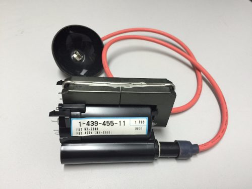
- The flyback transformer

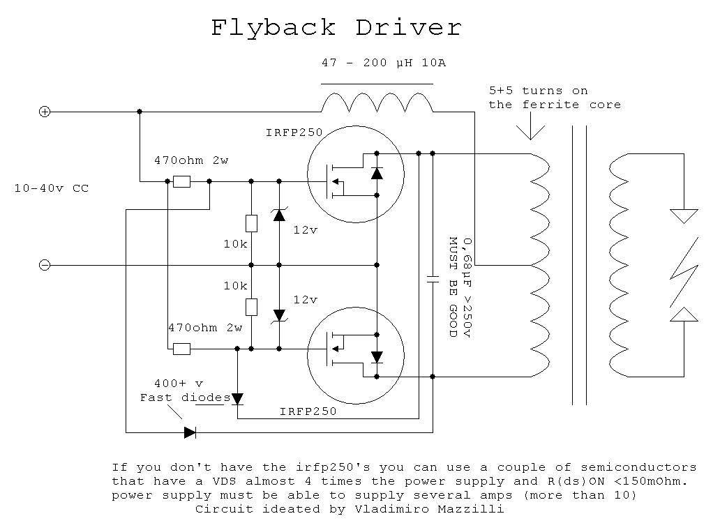
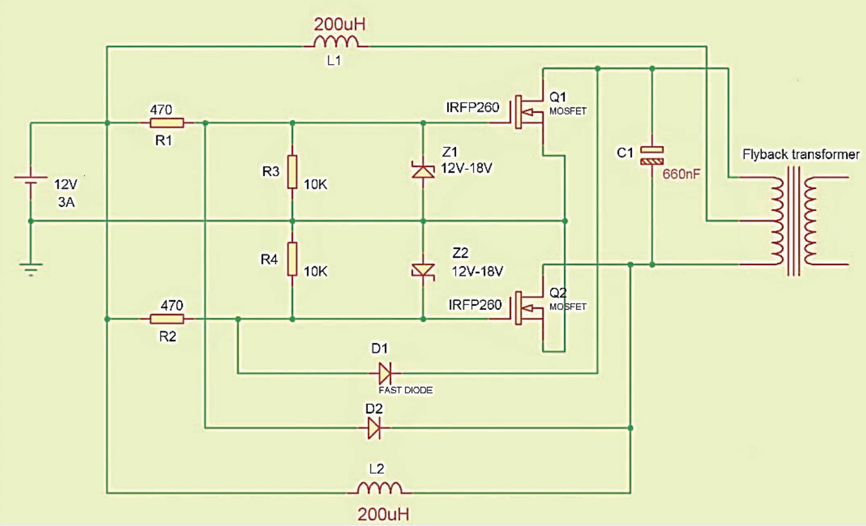
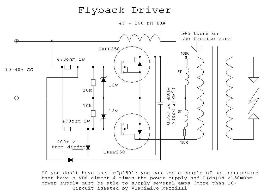
The switching circuit consists of a pair of IRFP250/260 MOSFETs and a pair of zener diodes that step up the 12 V d.c. 3A input into high frequency sinusoidal signals that drive the flyback transformer. The switching voltage which turns on and off the MOSFETs drops at a 660 nF capacitor rated at 1200 V and two 200 μH inductors which are parallel to the primary winding coil of the flyback transformer.
The operation is as follows:

Upon application of power, current flows through both sides of the MOSFET’s drains. One of the MOSFETs turns on faster than the other and more current draws to this MOSFET. This causes the other MOSFET to be turn off. The voltage starts to rise and fall sinusoidally. When Q1 turns on, the voltage at drain of Q1 will be ground while voltage at source of Q2 rises to a peak and drops back down during the one half cycle of LC tank. As the voltage of the source of Q2 drops to zero, the gate current to Q1 is also removed and as a result, Q1 turns off. This causes the drain voltage of Q1 to rise and Q2 turns on. The MOSFETs switch when there is least power induced. The same process repeats for the second half cycle. To prevent the oscillator from drawing huge peak currents and exploding, L1 is placed in series with the power supply functioning as a choke to mitigate current spikes. R1 limits the current that charges the gates to avoid damage of over current at the MOSFET. R3 of 10k pulls the voltage down to ground to avoid latchup. The Zener diodes regulates the voltage at 18 V. D1 and D2 ensures the gates voltage down to ground when the voltage on the opposite leg of the tanks is at ground.
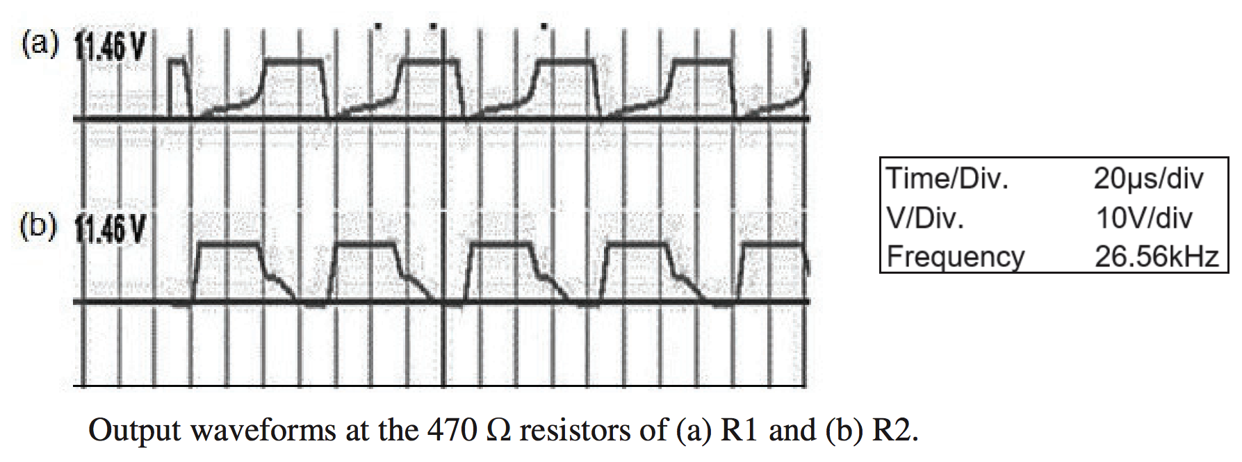
The waveforms at R1 and R2:

A DC ½ phase was observed at the pair of resistors. The peak
voltage of the half DC pulses dropped slightly to 11.46 V as a result of the zener diode regulation.
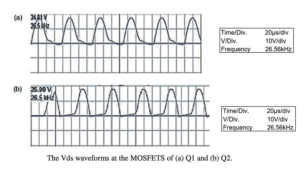
Half cycle sinusoidal signals alternatively oscillates at the drain-source (Vds) of the pair of IRFP260 MOSFET as shown in Fig. 4. The transistor is also an amplifier in the ZVS circuit for ensuring maximum power delivering to the next stage. Hence, fast switching transistor used was used. Each of the transistor connects to the inductor coil is mirrored to each other.
The waveforms of VDS of the MOSFETs:

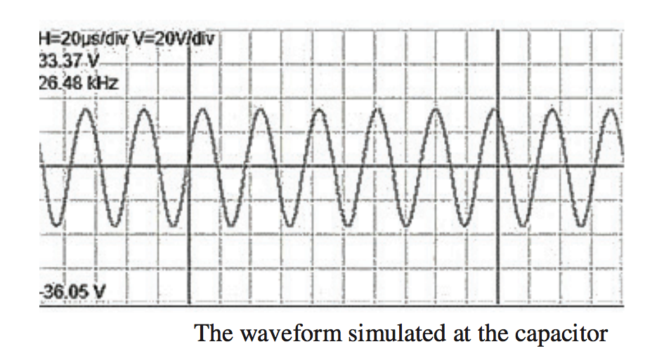
Finally the output of the switching circuit across C1,

Source: Zero Voltage Switching Driver and Flyback Transformer for
Generation of Atmospheric Pressure Plasma Jet
There is an improved version called the Andrinerii ZVS driver, which reportedly has a 30-35 % improvement in performance. This adds one pair of coils consisting of three turns (in the same direction as the primary1) in series with 100 Ω resistors. Each coil and resistor is added in parallel to each half of the primary coil, like so:

1 Otherwise the driver will be damaged.

