I'm designing a circuit with an ICF (indirect current feedback) amplifier, and am trying to calculate the gain of the resultant circuit.
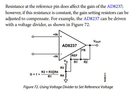
Using the AD8237 I followed the example here when designing with one modification. Instead of using a voltage follower, I used a resistor divider as the datasheet said I could (the ICF amplifier does not require a low impedance Vref like other 3 amp instrumentation amplifiers). Doing this does affect the gain, as can be seen from the snapshot from the datasheet below:
The gain when Vref = 0 is G = (1 + R2/R1). I tried dusting off some Thevenin equivalent circuit knowledge (it has been quite a while) and calculated the resistance with R1 removed and the voltage sources and calculated it as (R2 + R3||R4). Replacing R2 in the gain equation with this gives G = (1 + (R2 + R3||R4)/R1) which is the same as what is in the datasheet. So far so good!
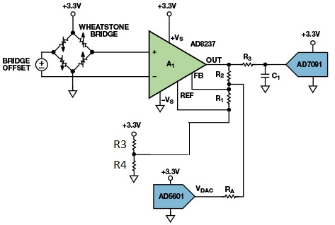
The challenge comes when adding the next part of the circuit - an offset voltage Vdac and resistor Ra as seen in the circuit below.
Doing the same as before, I calculated the resistance with R1 removed and all voltage sources shorted. From this I calculated it as (R3||R4 + R2||Ra) which when replacing R2 in the gain equation results in a gain of G = (1 + (R3||R4 + R2||Ra)/R1).
Is this the correct way of calculating this? Is the resultant gain I've calculated correct?
Edit: I don't think my math/understanding here is correct. I tried to derive equation (5) from the example as a check on my understanding and didn't have any luck. Can someone help me understand how that gain equation is being derived?
Many thanks!


