1
\$\begingroup\$

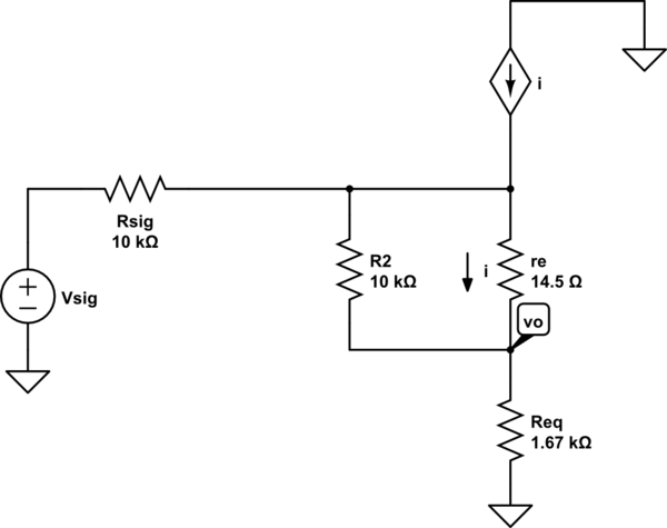
so I had my original circuit looking like below:

schematic

simulate this circuit – Schematic created using CircuitLab

I was able to simplify it to look like as follows:

schematic

simulate this circuit

but now am stuck. I don't know where to go from there. This is a small signal model for an amplifier utilizing an npn bjt. I'm being asked to find vo/vsig and Rin. Any help please??

\$\endgroup\$
6
  • \$\begingroup\$ Well you just use normal circuit analysis. Consider using node analysis to solve for an expression for \$V_o\$ \$\endgroup\$
    – user103380
    Commented May 30, 2018 at 3:16
  • \$\begingroup\$ Here you can find an example of a very similar circuit electronics.stackexchange.com/questions/372071/… \$\endgroup\$
    – G36
    Commented May 30, 2018 at 3:37
  • \$\begingroup\$ @G36 but this is for a mosfet. Mine is a npn bjt. There is current Ib flowing into the base. The mosfet doesn't have this problem. Can you provide an answer to this problem? Thank you \$\endgroup\$
    – JordenSH
    Commented May 30, 2018 at 3:44
  • 1
    \$\begingroup\$ but this is for a mosfet. Mine is a npn bjt Actually that doesn't matter much as these are small signal equivalent circuits, there's only an extra impedance between base and emitter that's not present for an NMOS. You talk about Ib flowing into the base, you should distinguish between the DC current Ib, which is irrelevant in these small signal equivalents and ib which is the small signal part of the base current. \$\endgroup\$ Commented May 30, 2018 at 7:23
  • 1
    \$\begingroup\$ You should include the original (large signal) schematic so that we're all clear what circuit we're talking about and that no mistakes were made in drawing the small signal equivalent. As it is, this small signal circuit just looks weird to me. \$\endgroup\$ Commented May 30, 2018 at 7:26

1 Answer 1

1
\$\begingroup\$

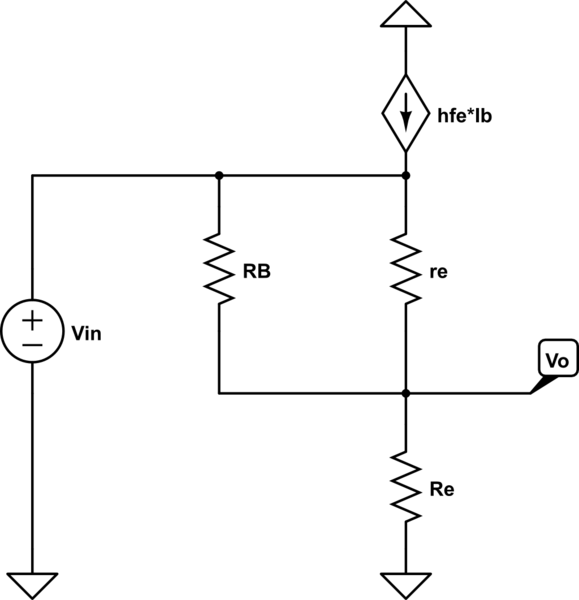
To make our life easier we can split the circuit (\$R_{sign} = 0\Omega\$) and analysis the bootstrap part first.
schematic

simulate this circuit – Schematic created using CircuitLab

As you can see we can find the voltage gain directly widout solving any equation. All we need is a voltage divider equation.

$$A_V = \frac{V_O}{V_{IN}} = \frac{R_E}{R_B||r_e + R_E} \approx \frac{R_E}{r_e+R_E}$$

You can find \$R_{IN}\$ by notice that:

\$I_{IN} = I_{R_B} + \frac{I_{r_e}}{\beta + 1}\$

And if you remember that \$r_\pi = (\beta+1)r_e\$ an that \$R_B\$ is in parrarel with \$r_\pi\$

We have

$$I_{IN} = (V_{IN} - V_O) \cdot \frac{R_B +(\beta+1)r_e}{R_B \cdot (\beta+1)r_e}$$

Aditional we know that \$Vo = V_{IN}\cdot A_V\$

$$I_{IN} = (1 - A_V) \cdot \frac{R_B+(\beta+1)r_e}{R_B \cdot(\beta+1)r_e}$$

And finally, we have

$$R_{IN} = R_B||(\beta+1)r_e \cdot \frac{1}{1 - A_V} = \frac{R_B||(\beta+1)r_e}{1 - A_V}$$

And here you find a different approach Effect of bootstrapping in amplifier circuit

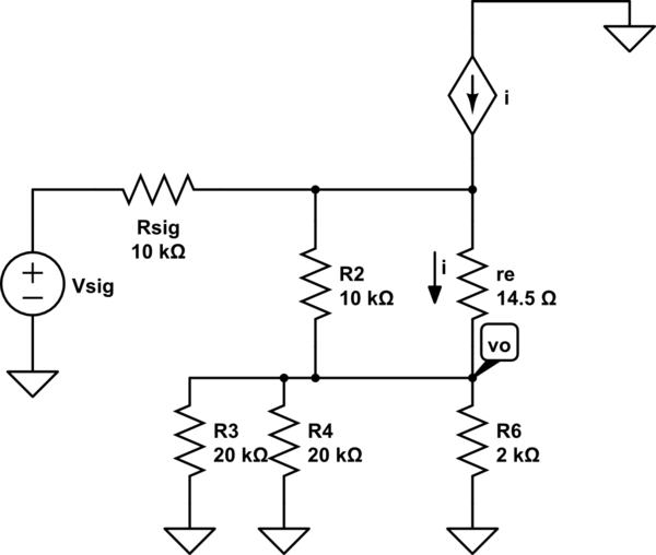
No back to your original circuit. The overall voltage gain is

$$A = \frac{R_{IN}}{R_{sig} + R_{IN}} \cdot A_V = $$
\$\endgroup\$

Your Answer

By clicking “Post Your Answer”, you agree to our terms of service and acknowledge you have read our privacy policy.

Not the answer you're looking for? Browse other questions tagged or ask your own question.