0
\$\begingroup\$

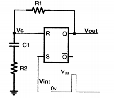
I'm trying to evaluate the time it takes the following mono-stable circuit to change the voltage of the capacitor from 1.25V to 2.5V after the Vin single pulse enters, and evaluate the recovery time of the circuit (given the voltage on the capacitor should be 5mV from zero for full recovery).

  1. In the official solution, the tau is calculated as \$\tau = (R1+R2)C1\$ while i thought it should be only \$R1\$.
    Why are both resistors taken into account? Isn't the charging voltage Vout charging only the upper side through R1?
    What happens in the discharging process? Again is it discharged through both of them?

  2. For the recovery time, the official solution states that after Q changes back from 1 to 0, the voltage in Vc drops from 2.5V to 1.25V (VDD=5V). I understand the the voltage on a capacitor should be continuous, but how did they calculate it?
    Is it because the change in the voltage for R2 is 1.25V, so that was the 'drop' in voltage there?
    Somehow I'm missing the point of calculating the voltage drop on the capacitors.

Many thanks!

Schematic

\$\endgroup\$
2
  • 1
    \$\begingroup\$ R1, C1, and R2 form a series RC circuit (assume no current into R terminal so open circuit) with the time constant in the solution. You can find more specific info about how it's charging/discharging here. You are basically just combining those two resistors in series. \$\endgroup\$ Commented Jun 1, 2018 at 6:39
  • \$\begingroup\$ Totally, simple RC circuit, don't know how i missed that. I've edited my question, Many thanks! \$\endgroup\$
    – DsCpp
    Commented Jun 1, 2018 at 6:47

2 Answers 2

1
\$\begingroup\$

Why both resistors are taken into account? Isn't the charging voltage Vout is charging the upper side only through R1?

If you neglected the reset pin (it's high impedance and with most logic series the current is in the uA range, so it can be neglected) and considered the entire impedance of the resistors and the capacitor on vout it would look like this:

\$ Z_{all} = Z_{r1} + Z_{c1} + Z_{r2}\$

Since this equation uses addition, if you wanted to find the charge time, it wouldn't matter which order these components were it (neglecting ESR of the cap), the charging time would be the same. If the resistors and capacitor were all in series and no reset pin, R1 and R2 could be combined into one resistor. However, you still need to have feedback for the reset pin, so don't do that.

\$\endgroup\$
0
\$\begingroup\$

The current flows through both resistors on both charge and discharge, so they both affect the capacitor charge rate. The resistance is split, in this case, to control the thresholds with a voltage divider between the cap voltage and the Q output.

This is much easier to visualize if you swap C1 and R2 in the above schematic. Since they're in series with no connection to the intermediate node, there will be no difference in the circuit behaviour; however, it's clear that R1 and R2 are b oth involved in the charge cycle, and that they form a voltage divider between V(C1) and Q0. In this way, the threshold analysis might be more intuitive.

\$\endgroup\$

Your Answer

By clicking “Post Your Answer”, you agree to our terms of service and acknowledge you have read our privacy policy.

Not the answer you're looking for? Browse other questions tagged or ask your own question.