2
\$\begingroup\$

in the application hints for an ADC (AD7927 page 26) it says:

The printed circuit board that houses the AD7927 should be designed such that the analog and digital sections are separated and confined to certain areas of the board. This facilitates the use of ground planes that can be separated easily. A minimum etch technique is generally best for ground planes as it gives the best shielding.

What do they mean by ground planes that can be seperated easily?

And what is a "minimum etch technique"?

\$\endgroup\$

2 Answers 2

4
\$\begingroup\$

"etch" here refers to "area etched free of copper"; in other words: the note recommends that you use ground planes as large as possible.

\$\endgroup\$
1
\$\begingroup\$

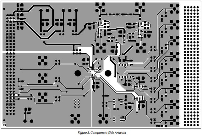
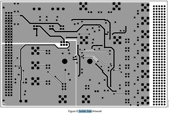
I refered the evaluation board for AD7927 i.e. EVAL-AD7927. I could answer your questios from that:

The printed circuit board that houses the AD7927 should be designed such that the analog and digital sections are separated and confined to certain areas of the board.

In picture below we can see that Analog and digital sections are separated and confined to certain areas instead of pouring copper wherever there are empty spaces

enter image description here

How that has helped in separating ground planes can be seen in below bottom layer picture. enter image description here

Thus I can understand that A minimum etch technique means using minimum etching on component side which helps for easy splitting of ground plane and better shielding.

\$\endgroup\$

Your Answer

By clicking “Post Your Answer”, you agree to our terms of service and acknowledge you have read our privacy policy.

Not the answer you're looking for? Browse other questions tagged or ask your own question.