0
\$\begingroup\$

I have a homework problem regarding differential amplifier.

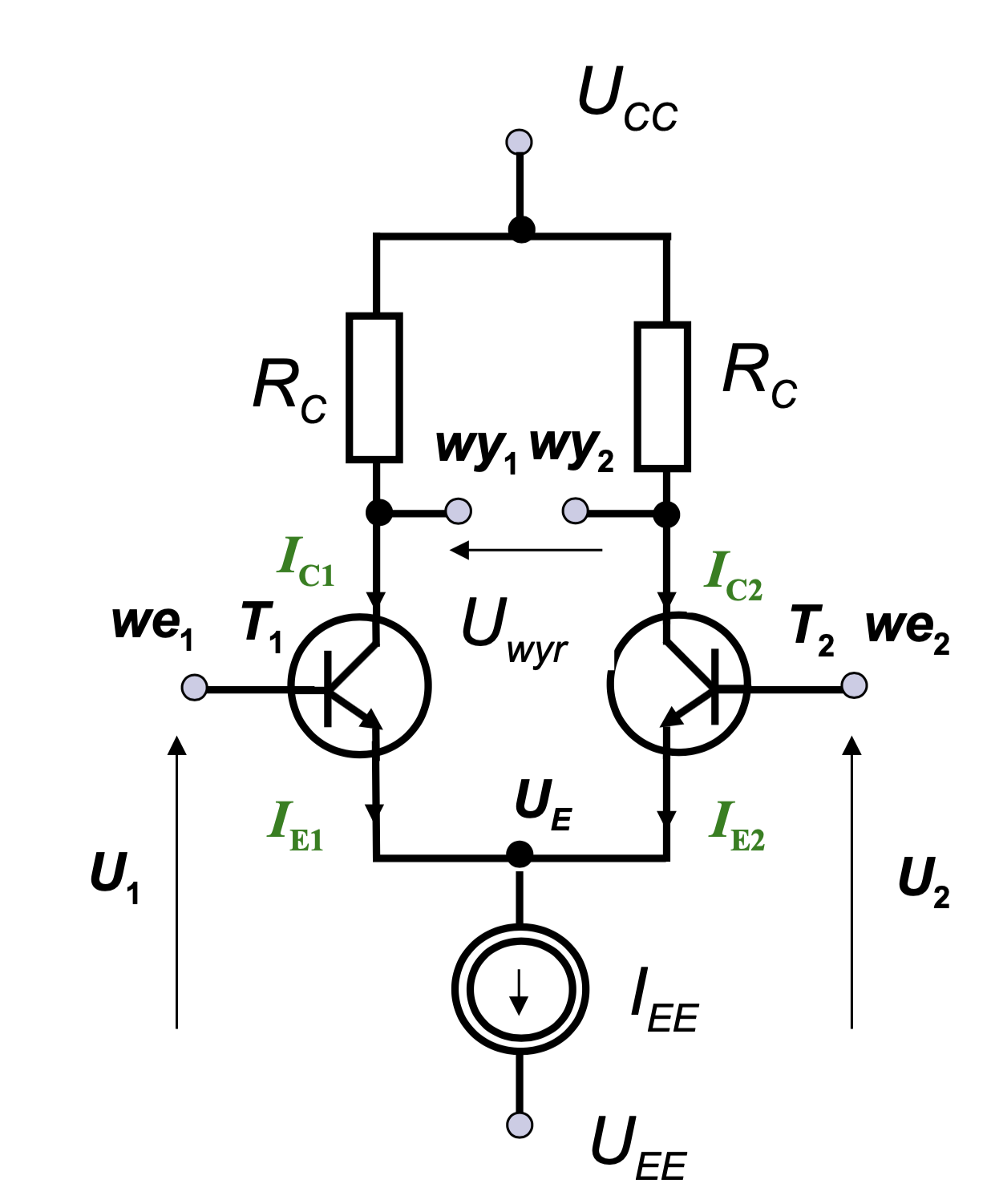
We have a differential amplifier with symmetric supply (i.e. \$V_{CC}=-V_{EE}\$). Emitters are connected to a perfect current source \$I_{EE}\$. T2's base is connected to the ground. T1's base (circuit's input) is connected to a sin wave generator, \$V_{PPUIN1}=2mV, \ \overline{V_{IN1}}=0V\$. We also know that \$\overline{V_{OUT2}}=8V, \ V_{PPOUT2}=400mV\$, where \$V_{OUT2}\$ is "wy2" in the image below. \$R_C=5k\Omega, \ V_{CESAT}=0.2V, \ V_{BE}=0.7V\$

  1. Calculate \$I_{EE}, \ V_{CC}\$
  2. \$V_{IN1}\$ was changed to \$-1V\$. Calculate \$V_{OUT1}, \ V_{OUT2}\$
  3. Draw the transfer characteristic for both outputs for \$V_{IN1}\in<-1V;1V>\$

enter image description here

Since \$U_{IN}=U_{IN1}<2\varphi_T\$, then we assume that both transistors are active. Hence we can use this formula (I am not familiar with English naming convention, so pardon me, if my guess is incorrect):

\$G_{DIFF2}=\frac{g_mR_C}{2}=\frac{I_{EE}R_C}{4\varphi_T}=\frac{V_{PPOUT2}}{V_{PPUIN1}}=\frac{400mV}{2mV}=200V/V\rightarrow I_{EE}=4mA\$

The average value at the second output is \$\overline{V_{OUT2}}=V_{CC}-\frac{I_{EE}R_C}{2}\rightarrow V_{CC}=18V\$

And now let's calculate for what \$U_{IN1}\$ T1 becomes saturated:

\$V_{CC}-I_{EE}R_C-V_{CES}=V_{IN1}-V_{BE}\\ V_{IN1}=-1.5V\$

so.. it seems like our assumption was wrong and both transistors are not active. But from the other side, if T1 is saturated, then T2 must be cut off... which does not make sense, since we were given the information, that there is a sine wave at the second output. At this point I don't know what to do next

\$\endgroup\$
11
  • \$\begingroup\$ Ale szkoła zaczyna się dopiero we wrześniu albo październiku, co to jakieś poprawki? \$\endgroup\$
    – G36
    Commented Aug 5, 2018 at 19:25
  • \$\begingroup\$ Is Vout2 = 8V a DC voltage at T2 collector? When Vin is 0V? \$\endgroup\$
    – G36
    Commented Aug 5, 2018 at 19:28
  • \$\begingroup\$ Also, notice that if Vin1 is -1V and T1 is TURN-ON the emitter voltage must be equal to -1.7V. So, the T2 Vbe voltage is Vbe2 = 0V - (-1.7V) = 1.7V. What this result tell us about T1 and T2? Do you know? \$\endgroup\$
    – G36
    Commented Aug 5, 2018 at 19:36
  • \$\begingroup\$ @G36 Robię sobie od czasu do czasu zadanka, aby nie zapomnieć tego przed egzaminem we wrześniu. 1) "Is Vout2 = 8V a DC voltage at T2 collector? When Vin is 0V?" yup 2) Hmm, I am not really sure, but, Ic(Vbe) and Uce(Vbe) characteristics tell us, that there will be big Ic2 current and T2 will be most likely saturated \$\endgroup\$
    – SantaXL
    Commented Aug 5, 2018 at 23:03
  • \$\begingroup\$ Yes indeed T2 will be in saturation if Vin1 = -1V. \$\endgroup\$
    – G36
    Commented Aug 6, 2018 at 12:59

1 Answer 1

1
\$\begingroup\$

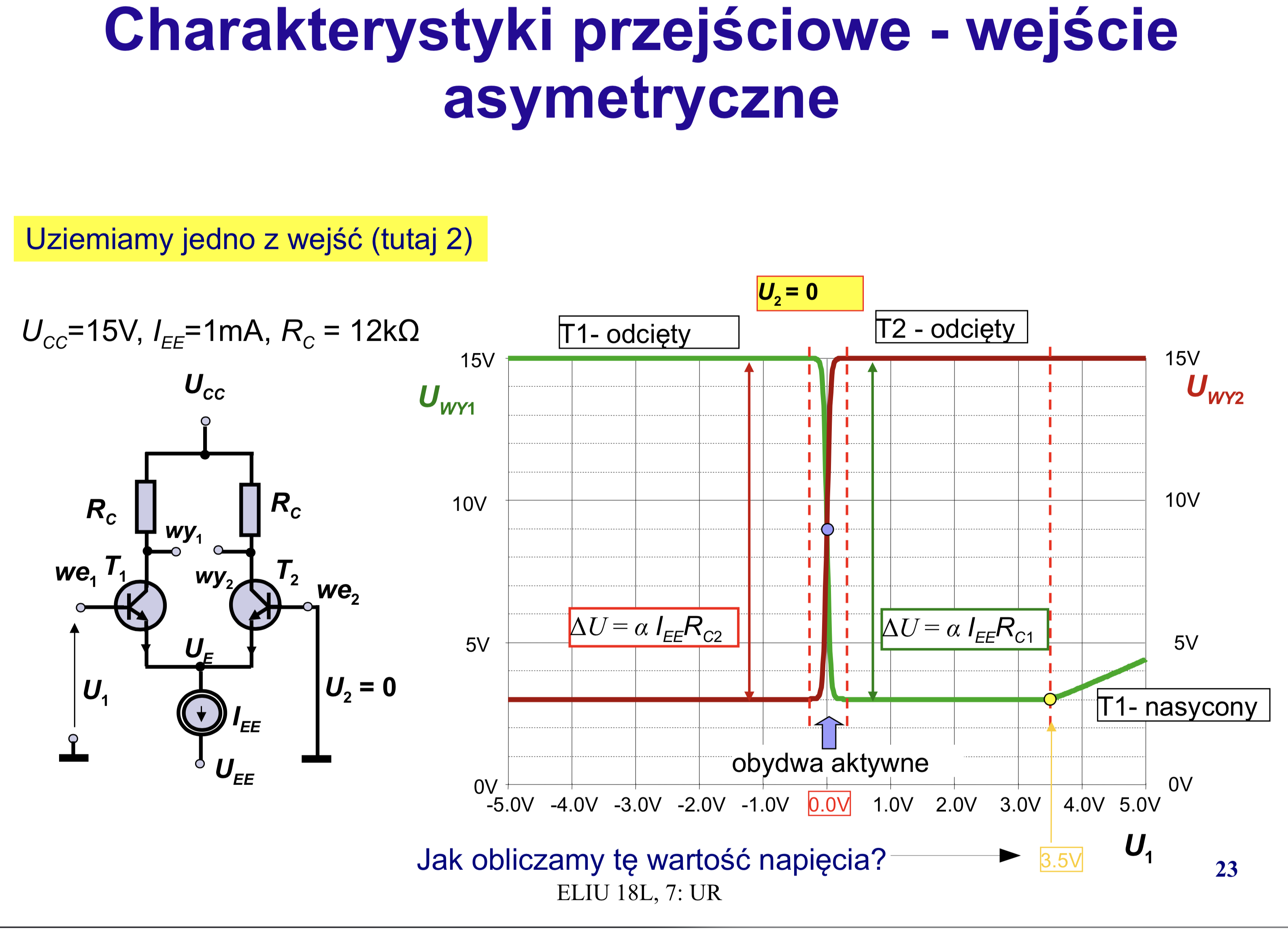
I am afraid you (we) were wrong here. Just take a look at this

enter image description here

As you can see from the diagram we have:

\$V_{CC} = 15V, I_{EE} = 1\textrm{mA}, Rc = 12\textrm{k}\Omega \$

And as you can see from the transfer characteristic the output voltage at the \$T_2\$ collector is equal to \$3V\$ for \$-1V\$ at the input (T1 base).

\$V_{out2} = 15V - 1\textrm{mA}\cdot 12\textrm{k}\Omega = 3V\$

And also notice that \$T_2\$ is not in the saturation region in this case.

Because while \$T_2\$ collector is at \$3V\$. The \$T_2\$ base is at \$0V\$ Therefore, the base-collector junction is reverse biased.

And the emitter voltage is around \$-0.7V\$ and \$V_{CE2} = 3V - (-0.7V) = 3.7V\$

And we can easily calculate the point at which \$T_1\$ transistor enters the saturation region. For example, if we assume \$V_{CE2(sat)}=0.2V, \ V_{BE}=0.7V\$ we can solve for the minimum voltage needed at the input to saturated the \$T_1\$ transistor.

\$U_{1(sat)} = 3V - 0.2V + 0.7V = 3.5V\$

And I hope that this does not need any further explanations?

But let me back to your current problem and this question:

  1. \$V_{IN1}\$ was changed to \$-1V\$. Calculate \$V_{OUT1}, \ V_{OUT2}\$

In this circuit, we have \$ V_{CC}=18V, Rc = 5 \textrm{k}\Omega, I_{EE} = 4\textrm{mA} \$

It should be clear for you that such a large negative voltage at the \$T_1\$ base will cut-off \$T_1\$ and allows all the \$I_{EE}\$ current to flow through the \$T_2\$ transistor (T1 cannot be a turn-on because this would cause a very large voltage across T2 base-emitter junction).

If so, the voltage at the \$T_2\$ collector is:

\$V_{OUT2} = 18\textrm{V} - 4\textrm{mA}\cdot 5\textrm{k}\Omega = -2\textrm{V}\$

But notice that the \$T_2\$ base is at \$0V\$ and \$T_2\$ emitter voltage is at \$-0.7V\$.

And the collector-emitter voltage is \$V_{CE2} = -2V - (-0.7V) = -1.3V\$

But in NPN transistor we cannot have a negative voltage between collector and emitter (collector voltage cannot be lower than the emitter voltage).

So, this result tells us that our BJT (\$T_2\$) is in saturation region for \$-1V\$ at the input.

Therefore:

\$V_{out2} = V_{E2} + V_{CE(sat)} = -0.7+0.2V = -0.5V\$

And the \$T_2\$ collector current is

\$ I_{C2(sat)} = \frac{V_{CC} - V_{out2} }{R_{C2}} = 3.5\textrm{mA}\$

The base current is \$I_{B2} = I_{EE} -I_{C2(sat)} = 4\textrm{mA} - 3.5\textrm{mA} = 0.5\textrm{mA} \$

I hope that this explains why \$T_2\$ is indeed in the saturation region for \$-1V\$ at the input (T1 base). Because here we have a different situation than shown in your example transfer characteristic.

\$\endgroup\$
10
  • \$\begingroup\$ Thank you for this answer. Yes, it does indeed explain why \$T_2\$ is saturated for this voltage. However, I have another problem (3rd point of my OP). To be specific: \$T_2\$ will be in saturation region until \$I_{C2}\$ becomes smaller than \$I_{C2(sat)}=3.7mA\$. So the question, when this will happen? Well, when \$I_{C1}>0.3mA\$ but I don't know how to calculate this, i.e. \$V_{CC}-I_{C1}R_C-V_{CE1}=V_{IN1}-V_{BE}\$ but I don't know what \$ V_{CE}\$ will be equal to. All I know is that \$V_{IN1}\$ will be somewhere between \$<-2\varphi_T;0V>\$ \$\endgroup\$
    – SantaXL
    Commented Aug 16, 2018 at 22:53
  • \$\begingroup\$ Or maybe should I use such formula? But it seems to me a bit too hard, it is just a typical test (kolokwium) imgur.com/a/XFwa0Gt \$\endgroup\$
    – SantaXL
    Commented Aug 16, 2018 at 23:01
  • \$\begingroup\$ @SantaXL Unfortunately, you have to need to assume Vce(sat) = 0.2V or use this "hard" formula. How did you find Ic2(sat)=3.7mA? \$\endgroup\$
    – G36
    Commented Aug 17, 2018 at 15:43
  • \$\begingroup\$ your calculation is incorrect, Vcc=18V, Vout2 =-0.5V, Rc2=5k, hence 18.5/5k=3.7mA. But that's just a detail \$\endgroup\$
    – SantaXL
    Commented Aug 17, 2018 at 19:53
  • 1
    \$\begingroup\$ @SantaXL Looks good \$\endgroup\$
    – G36
    Commented Aug 19, 2018 at 9:35

Your Answer

By clicking “Post Your Answer”, you agree to our terms of service and acknowledge you have read our privacy policy.

Not the answer you're looking for? Browse other questions tagged or ask your own question.