2
\$\begingroup\$

Upfront, I apologize if this may be a terribly obvious question. I don't have all of the background to understand it confidently.

I'm trying to apply a voltage for an electrophoresis experiment across a glass capillary, which eventually meets a silicon microchip that serves as an optical detector. I need to be able to ground the capillary voltage either before or at the microchip surface in order to avoid having a floating chip, which generates signal that is difficult to interpret.

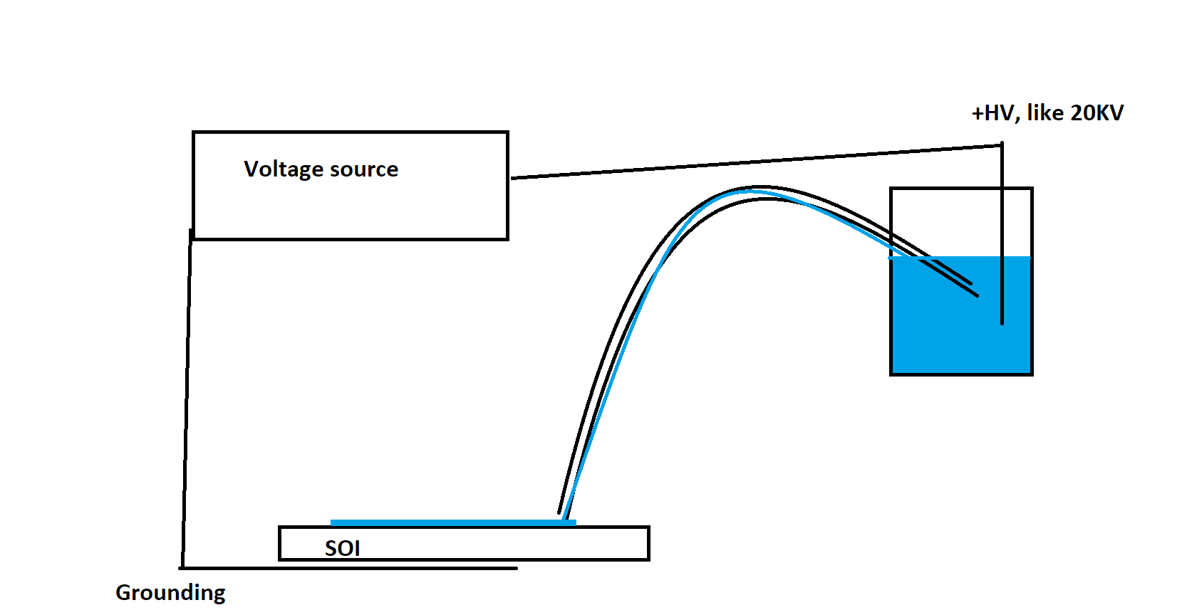
My question is whether or not I can ground my microchip by applying a piece of conductive tape to the bottom, which would lead to my grounding electrode. The high voltage electrode would be placed on the other end of my capillary, in solution. My concern is that because the chip is technically silicon-on-insulator, the circuit may be incomplete. The capillary is filled with the same liquid, so there should be a conductive path from chip surface to HV electrode. But I wonder if it'll just happen to work anyway, or if I'm missing something that would allow it to work.

Here's a very rough schematic of what I'm looking at. enter image description here
Thank you very much for your help.

\$\endgroup\$
3
  • \$\begingroup\$ wait, is your 20kV shorted to ground? That seems like a recipe for disaster \$\endgroup\$
    – Hearth
    Commented Nov 5, 2018 at 16:26
  • \$\begingroup\$ Oh, no. They're both connected to the voltage source. Definitely not shorted together. \$\endgroup\$
    – user168273
    Commented Nov 5, 2018 at 16:27
  • \$\begingroup\$ Your schematic shows them shorted together. Your schematic is very unclear in general; it might be a good idea to use the schematic editor this site provides. It's the little circuit diagram with a pencil when you go to edit your question. \$\endgroup\$
    – Hearth
    Commented Nov 5, 2018 at 16:29

2 Answers 2

2
\$\begingroup\$

No. With SOI, grounding the back of the substrate has no effect. The silicon on top will have to be designed with an explicit grounding path.

\$\endgroup\$
0
\$\begingroup\$

Your schematic is unclear, so I can't really ascertain where are those 20kV being referenced to.

SOI (Silicon On Insulator) technology uses an insulating substrate, so connection to the substrate would not do anything.

If the insulation layer is thin enough 20kV could be enough to break it down and destroy the IC. On Silicon On Sapphire technology just ~1mm of substrate should be enough to sustain this potential.

An alternate SOI technology, trench insulation with buried silicon dioxide layers, is similar but more compatible with the standard IC fabrication process and thus more common. But here the actual substrate is still a conductive silicon wafer although the active areas will be insulated from it. 20kV would surely break it down.

However, if that SOI-IC is actually floating and referenced to 20kV, you have to be very careful on how you deal with your grounds.

\$\endgroup\$
2
  • 1
    \$\begingroup\$ SOI that I have used normally only has a ~1 um buried oxide layer as the insulator. The bulk material is an ordinary silicon wafer. \$\endgroup\$
    – Evan
    Commented Nov 5, 2018 at 19:54
  • \$\begingroup\$ @Evan that's what I was referring to as trench insulation. When I think SOI I explicitly think of Silicon on Sapphire. I will edit to clarify. \$\endgroup\$ Commented Nov 5, 2018 at 20:01

Your Answer

By clicking “Post Your Answer”, you agree to our terms of service and acknowledge you have read our privacy policy.

Not the answer you're looking for? Browse other questions tagged or ask your own question.