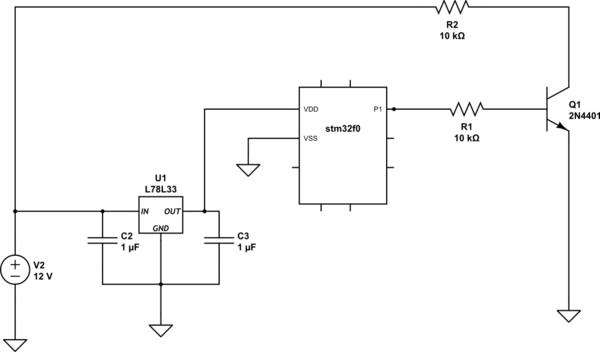
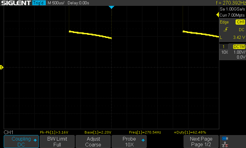
I suspect that resistor R1's value is too large; it is preventing transistor Q1 from being driven into saturation. From the oscilloscope trace it appears Q1 is operating in forward active mode (small signal amplifier mode), not saturation mode.
To confirm this, connect one oscilloscope probe at Q1's base, connect a second oscilloscope probe at Q1's collector, and use the oscilloscope's MATH function to calculate and display the difference \$V_B - V_C\$. The hallmark for BJT saturation is the transistor's base-collector diode is "forward biased" (i.e., \$V_{BC} > 0\,\mathrm{V}\$). My hunch is you'll measure \$V_{BC}<0\,\mathrm{V}\$, meaning the transistor is not achieving saturation.
(NB: Connect each oscilloscope probe's ground lead to your circuit's ground node.)
To solve for R1's value, try the following process.
- Determine the transistor's collector current when the transistor is saturated, \$I_{C(sat)}\$.
(NB: The load is in series with the transistor's collector; therefore, the load current—whatever it is—is \$I_{C(sat)}\$.)
(NB: Estimate \$V_{CE(sat)}\$'s value from the 25°C curve shown in Fig. 4 "Collector-Emitter Saturation Voltage vs. Collector Current" in this 2N4401 datasheet published by ON Semiconductor.)
$$
I_{R2} = I_{C(sat)} = \frac{V_{R2}}{R2} = \frac{V_{CC}-V_{CE(sat)}}{R2} \approx \frac{V_{CC}}{R2}
$$
Determine the transistor's forward current gain when operating in saturation mode, \$\beta_{sat}\$.
(NB: For small signal transistors, \$\beta_{sat}=10\$ is common. See Fig. 4 and Fig.5 in this 2N4401 datasheet published by ON Semiconductor.)
Calculate the required current into Q1's base to saturate Q1, \$I_{b(sat)} = I_{C(sat)}/\beta_{sat}\$
:: CHECK :: Ensure your microcontroller's digital input/output (DIO) pin can safely source a current of \$I_{B(sat)}\$ when the pin is configured as an OUTPUT and is programed to produce a logic HIGH output signal.
A digital logic HIGH signal can be any voltage between \$V_{OH}\le V_{HIGH} \lt V_{CC}\$ where \$V_{OH}\$ is the minimum voltage for a logic HIGH output signal. Use the microcontroller's datasheet to determine \$V_{OH}\$'s value.
(NB: See also the webpage "Logic Levels" on SparkFun's website.)
Use the transistor's data sheet to determine the base-emitter voltage when the transistor is operating in saturation mode \$V_{BE(sat)}\$ with a current of \$I_{C(sat)}\$ flowing in its collector.
(NB: Estimate \$V_{BE(sat)}\$'s value from the 25°C curve shown in Fig. 5 "Base-Emitter Saturation Voltage vs. Collector Current" in this 2N4401 datasheet published by ON Semiconductor.)
Use Ohm's Law and Kirchoff's Voltage Law to calculate R1's value:
$$
R1 = \frac{V_{R1}}{I_{R1}}
= \frac{V_{OH}-V_{BE(sat)}}{I_{B(sat)}}
$$
- Using your calculated value for R1, choose R1's component value from a table of standard resistor values (example table).
Some additional comments.
Add a weak pull-down resistor (perhaps \$10\,\mathrm{k\Omega}\$) between the MCU's DIO pin and ground (to the left of resistor R1). This resistor's job is to keep transistor Q1 turned OFF (in cutoff) when the MCU is not actively driving a voltage at its DIO pin—e.g., when power is initially applied to the system and the microcontroller's DIO pins are initially configured as inputs.
In your figure, R2 is shown as a \$10\,\mathrm{k\Omega}\$ resistance. If \$10\,\mathrm{k\Omega}\$ is the actual load resistance—i.e., if the current through the load is around \$1\,\mathrm{mA}\$ when the load is energized, then by my calculations \$R1=10\,\mathrm{k\Omega}\$ should suffice to saturate Q1. The oscilloscope trace shows Q1 is not saturating, so my suspicion is the \$10\,\mathrm{k\Omega}\$ resistance value shown for R2 is not the load's actual resistance.


