0
\$\begingroup\$

Hello I am in need of some advices, I am planning on placing a power switch for my circuit that uses 12v 2A DC. But unfortunately i could not find a switch with the form factor needed that is rated for that power. So what i initially planned is to use a N - channel mosfet along with the switch. This make lower rated switch be able to switch the load. As shown
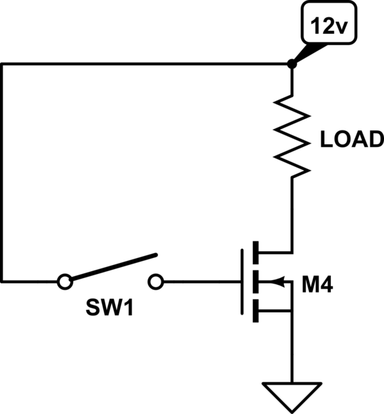
schematic

simulate this circuit – Schematic created using CircuitLab

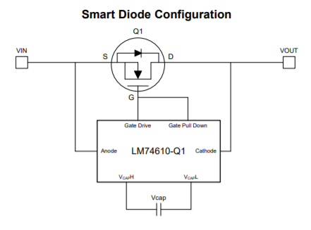
But I already have a reverse voltage protection IC LM74610 that utilizes a N-channel mostfet to switch to the load.

enter image description here

It would be kind of redundant if i use 2 mostfet switches, So i was thinking if anybody can help me modify the example circuit of the LM74610 to combine with a switch.

I would logically assume that it would be placed at the gate drive pin but before gate pull down. It is my first time dealing with ic that are not referenced to ground so im not really sure.

\$\endgroup\$
2
  • 1
    \$\begingroup\$ wrong way ..put load on drain \$\endgroup\$
    – D.A.S.
    Commented Mar 18, 2020 at 18:03
  • \$\begingroup\$ @TonyStewartSunnyskyguyEE75 thank you for pointing that out, i have edited the schematics. Now that you mention it, the LM74610 is using it differently too, power enters the SOURCE to the DRAIN \$\endgroup\$
    – Jake quin
    Commented Mar 18, 2020 at 18:31

1 Answer 1

2
\$\begingroup\$

You cannot manipulate the gate control of the LM74610 such that the mosfet will not conduct, because the body diode of the mosfet will always be conducting (in case of correct polarity).

You need the apply a second mosfet to switch on the circuit: either like you suggested or e.g. using mosfets back-to-back and e.g. the LTC4359 as alternative for the LM74610.

\$\endgroup\$
6
  • \$\begingroup\$ Looks like back to back diode it is then, If you dont mind i ask, Here was my anology why i think it should have worked. The logic of the RVP ic is it turns on/ off the mosfet, And according to the datasheet the gate drive is pulled to the anode, which would turn on the mosfet during correct polarity, for incorrect polarity the gate of the mosfet is pulled down via the pulldown pin of the ic thus preventing the cuircuit from being completed. So theoretically if i add a switch between the gatedrive pin of the ic and the gate of the mosfect, . . . . \$\endgroup\$
    – Jake quin
    Commented Mar 18, 2020 at 20:14
  • \$\begingroup\$ so the gate of the mosfet is being "tricked" that it has no voltage because the switch is disconnected. If you can point out where the analogy went wrong. it would greatly help in my future endevours. \$\endgroup\$
    – Jake quin
    Commented Mar 18, 2020 at 20:16
  • \$\begingroup\$ Your writing about turning of the channel of the mosfet is correct. But a mosfet has a parasitic element: its body diode. You cannot turn on/off this body diode. It is always there and in this application is it forward biased and therefore always conducting (with correct polarity). \$\endgroup\$
    – Huisman
    Commented Mar 18, 2020 at 20:41
  • \$\begingroup\$ The back-to-back implementation puts the body diodes such that always one body diode is forward biased and the other is reversed biased, so, there is always one blocking the 'parasitic conduction' \$\endgroup\$
    – Huisman
    Commented Mar 18, 2020 at 20:46
  • \$\begingroup\$ oh i see and lastly, why is it that the n channel is kinda inverted, where the source is the one connected to the positive end and the drain is to the negative end. I understand from the data sheet why use an NMOS but as to why its inverted \$\endgroup\$
    – Jake quin
    Commented Mar 18, 2020 at 22:42

Your Answer

By clicking “Post Your Answer”, you agree to our terms of service and acknowledge you have read our privacy policy.

Not the answer you're looking for? Browse other questions tagged or ask your own question.