According to the Wikipedia page for common emitter amplifiers, the addition of an emitter resistor decreased the gain of the circuit. However, to me it appears that if the resistor was omitted, then V_out would be approximately equal to the ground mode (when the transistor is conducting). But when the resistor is present, V_out would be equal to the drop across the resistor. Why then does the resistor reduce the gain? Please note I am very new to transistor circuits, and to electronics in general.
-
\$\begingroup\$ Do you understand the emitter follower or common collector circuit. If not, study it then re-ask your question. \$\endgroup\$– Andy akaCommented Mar 31, 2020 at 8:14
-
\$\begingroup\$ The gain of a common emitter amplifier is approximately -Rc/Re where Rc is the collector resistor and Re is the emitter resistor. So the smaller Re is, the higher the gain. The larger Re is, the smaller the gain. For a given Rc. Now, if you don't see why the gain is approximately -Rc/Re, then just read about the common emitter amplifier to understand that. \$\endgroup\$– user57037Commented Mar 31, 2020 at 9:28
-
\$\begingroup\$ Have a look at khanacademy.org/science/in-in-class-12th-physics-india/… (Hindi accent) and en.wikipedia.org/wiki/Common_emitter \$\endgroup\$– skveryCommented Mar 31, 2020 at 10:43
-
\$\begingroup\$ I am really surprised: The second link as given above (wikipedia) contains the following statement: Emitter degeneration with RE would not be identical with negative feedback because it would not influence bandwidth and output resistance. Unbelievable!! \$\endgroup\$– LvWCommented Mar 31, 2020 at 14:35
-
1\$\begingroup\$ Maybe the whole problem is confusion around what is meant by "gain?" Often people think of beta as gain. At a given operating point, beta does not change, and external components don't affect beta, or at least not directly (maybe by shifting the operating point). Once you understand that in a common emitter amplifier, the gain is Vout/Vin, with Vout being taken at the collector, and Vin being at the base, then it may make more sense. \$\endgroup\$– user57037Commented Mar 31, 2020 at 17:26
5 Answers
It's useful to think of a transistor operating in three modes, cut off, linear, and saturated.
When cut off, the collector current is zero. When saturated, the base current is high, and VCE is small. These are the two modes when using a transistor as a switch. You appear to be thinking of the saturated mode in your question.
Wikipedia is talking about the linear, or amplifying mode, where the collector current is beta times the base current, and VCE is a few volts.
Gain is the output voltage change divided by the input voltage change.
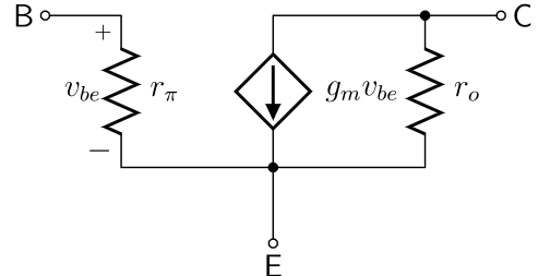
In the small signal hybrid pi model the collector current changes proportional to the change in base voltage (relative to the emitter) so there is a voltage change at the collector proportional to the load resistance (parallel with ro).
If you add an emitter resistor, the base-emitter voltage does not change as much so the current change is less and therefore the gain is reduced. That is because the emitter current change causes the emitter voltage to change in the same direction as the change in base voltage, partially counteracting the effect.
In a common-emitter amplifier, think of the transistor as a variable resistor controlled by the base current (\$i_b\$):
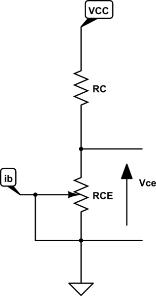
simulate this circuit – Schematic created using CircuitLab
The output voltage (and thus the voltage gain) is determined by the voltage across the variable resistor (i.e. \$V_{ce}\$).
Now put a resistor between the low-end of the variable resistor and the GND:
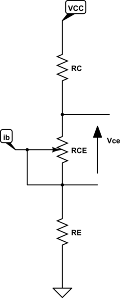
For the same VCC, the voltage across the variable resistor drops due to the increased total resistance. So the output voltage (determined by the voltage across the variable resistor) drops and so does the gain.
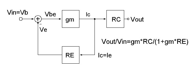
The emitter resistor causes negative feedback. This can be shown using a block diagram based on the classical formulas for describing the input-output relations. It is a well-known fact that negative feedback reduces the gain factor. This is - in most cases (opamp) - a desired result of negative feedback.
Note that the output current Ic is determined by the input voltage Vbe via the transconductance gm=d(Ic)/d(Vbe). (In the block diagram I have used the commonly used simplification Ic=Ie; all voltages and currents are small-signal quantities and not DC values).
The gain formula shows how the resistor RE reduces the gain. More than that, you can see that the simplification Vout/Vin=RC/RE (as mentioned in one answer) is applicable for RE>>1/gm only.
Comment 1: Because the signal output voltage across the collector resistor RC is referenced to common ground - and NOT to the supply voltage - there is a sign inversion between input and output voltages which is not contained in the block diagram (the block RC should habe a negative sign).
Comment 2: It is easy to explain in words how feedback reduces gain. An increase of the input voltage Vb (at the base node) causes an increase in Ie which in turn also increases the voltage across RE. Hence, the emitter voltage Ve goes up and reduces Vbe (if compared with Ve=fixed at ground for RE=0). Hence, the Vbe increase is smaller than the input signal (Vb) increase - and the Ic increase is remarkably smaller if compared with the case RE=0.
(I like to add, that the block diagram and the corresponding explanation of the feedback effect proove again that the BJT is a voltage-controlled device Ic=f[exp(Vbe/Vt)] .)
Consider the following circuit.
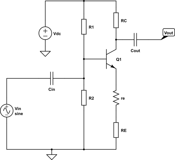
simulate this circuit – Schematic created using CircuitLab
In this circuit Q1, R1, R2, RC, RE, Cin and Cout represent real components.
re represents the intrinsic impedance of Q1. \$ re \approx \dfrac{25}{I_C} \$ ohms if \$ I_C \$ is in mA at room temperature.
The usual design procedure is to pick a quiescent \$ I_C \$ and choose RC such that \$ V_C \$ is half Vdc at this current to maximise voltage swing at the output.
Now if we assume \$ h_{fe} \$ is large Then \$ I_C \approx I_E \$ So the gain is \$ \dfrac{RC}{RE + re} \approx \dfrac{RC}{RE} \$ if re is small relative RE.
I usually play with RC and RE to get nice standard values. Since we know the quiescent \$ I_E \$ we know \$ V_E \$ and we want \$ V_B \$ to be approximately 0.6V higher than this. knowing \$ I_B = \dfrac{I_C}{h_{fe}} \$ we can choose R1 and R2, The current in R1 should be large compared with \$ I_B \$ so it does not vary. I usually go with ten times \$ I_B \$ with maximum \$ h_{fe} \$ as a rule of thumb.
Finally we can choose Cin and Cout to have a low impedance at the minimum frequency of interest.
-
\$\begingroup\$ Warren Hill....In your drawing I see the classical transistor symbol and - in addition - an external quantity re (which is nothing else than the inverse of gm). But gm is the TRANCCONDUCTANCE gm= d(Ic)/d(Vbe) which constitutes the INTERNAL connection (conversion) between input voltage and output current of the BJT. For my opinion, it is not correct to use the traditional symbol for a BJT and - in addition - an external resistance re. \$\endgroup\$– LvWCommented Mar 31, 2020 at 13:58
-
\$\begingroup\$ HI @LvW but re is re = d(Vbe)/d(Ie) \$\endgroup\$– G36Commented Mar 31, 2020 at 14:10
-
\$\begingroup\$ More than that, we can MODEL the role of gm=1/re using a resistor symbol in an small-signal EQUIVALENT circuit diagram - however, it must not be called "intrinsic impedance" because it is neither an impedance nor a resistance. And we must not use it in "classical" circuit diagram which contains real elements - and not differential (dynamic) quantities. In your drawing, a DC curent would cause a voltage drop across re which is not the case. \$\endgroup\$– LvWCommented Mar 31, 2020 at 14:10
-
\$\begingroup\$ G36...it is a differential quantity called transconductance - if you define it as d(Vbe)/d(Ie) or d(Vbe)/d(Ic). It does not matter. Such a quantity must not appear in a circuit diagram. It is one of the basic rules of circuit diagrams to clearly discriminate between (a) diagrams containing real parts ands (b) equivalent small signal diagrams (without DC relevance). \$\endgroup\$– LvWCommented Mar 31, 2020 at 14:13

