0
\$\begingroup\$

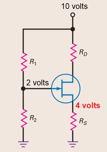
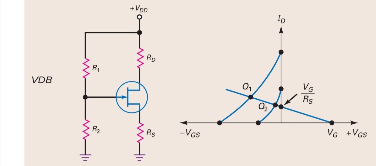
I already know how Gate-bias, Self-bias, and Current-source bias works in a JFET configuration. However, I am still stuck in voltage-divider-bias JFET circuit. (circuit below)

In a JFET circuit, the gate-source voltage must be reverse-biased. However, in a VDB JFET circuit, the gate voltage is always positive.

Posted below is also the transconductance curve, it shows that the Q point in this VDB circuit will have a negative voltage at either Q1 or Q2, how is that suppose to happen if VDB produce positive voltage at the gate?
\$\endgroup\$

1 Answer 1

1
\$\begingroup\$

it shows that the Q point in this VDB circuit will have a negative voltage at either Q1 or Q2, how is that suppose to happen if VDB produce positive voltage at the gate?

I think you are getting confused between the absolute voltage at the gate with respect to ground (0 volts) and the voltage between gate and source. Consider this scenario: -

enter image description here

With 2 volts applied to the gate node, current will start to flow into the JFET drain and raise the source voltage thus cutting-off the channel. Equilibrium will be found with a source voltage (with respect to ground) that is more positive than the gate voltage with respect to ground i.e. \$V_{GS}\$ is negative a couple of volts for instance.

\$\endgroup\$

Your Answer

By clicking “Post Your Answer”, you agree to our terms of service and acknowledge you have read our privacy policy.

Not the answer you're looking for? Browse other questions tagged or ask your own question.