0
\$\begingroup\$

I want to design an amplifier which works in 20kHz-100kHz range with 0.1V peak to peak signal.

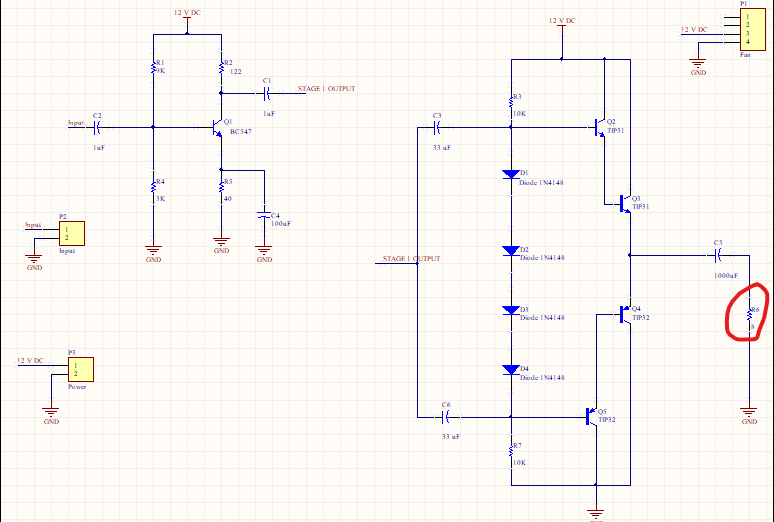
This is my circuit.

It works fine in the simulation. It works fine without connecting R6 8 ohm load. But when I connect the 8 ohm load output signal get distorted.

How can I solve this problem?

my circuit

\$\endgroup\$
3
  • 3
    \$\begingroup\$ What sort of distortion? Does it go wrong at the zero-crossing points? Are sine waves clipped? Does it show extra frequencies? \$\endgroup\$ Commented Oct 22, 2020 at 13:07
  • 2
    \$\begingroup\$ This will have copious amounts of crossover distortion. LM1875 costs $2. \$\endgroup\$
    – bobflux
    Commented Oct 22, 2020 at 13:10
  • \$\begingroup\$ Its more like extra frequencies added to normal sinusoidal signal. \$\endgroup\$
    – jan411
    Commented Oct 23, 2020 at 14:52

3 Answers 3

1
\$\begingroup\$

Try lowering the values of the 10k resistors ( R3 & R7). The 10k values may not be able to supply enough base current to the driver transistors.

\$\endgroup\$
0
\$\begingroup\$

Imbalance of base-drive will cause different voltages across the DC_blocking capacitors. Examine the voltages at bases of your 2 Darlingtons.

\$\endgroup\$
0
\$\begingroup\$

This can be easily solved with NFB (neg.feedback) using an Op Amp with some low gain but adequate GBW or a better CE amplifier with RC feedback from the output to the input with a series R added from source to achieve about half of the expected gain from R ratios. also adding Re=5 improves THD yet reduces gain to 112/5. Define desired gain better to choose.

Consider Rs=100 added or included and 2k for NFB from output to cap to base for a maybe gain of 10.

Each TIP on the datasheet has an hFE = 25 typ. @ 3A and approx =130 @ 3A/25A or a net gain of In order to have high Damping factor >>100 the Zout must be <<1% of the 8 ohm load.

  • since 2 stages only yields a total hFEt=3250 x 8 ohm load , Req= 8*3250 = 26k for maximum power transfer, but for damping the source impedance must be <<1% of this or 260 ohms which is near the open loop Rout of many Op Amps.
    • Your CE amp has an output R=122 ought to be OK
  • But with NFB using the inverting feedback of an Op Amp this can be reduced by Gain.
  • Stray capacitance can cause loss of phase margin so an RC snubber is used to attenuation potential oscillations at low gain.
  • so choice of Op Amp with high GBW is preferred for fmax in your passband is desirable, e.g. >=10MHz and Av=<10?

Then your crossover distortion reduces by amount feedback gain e.g. 10MHz/100kHz/Av=10=10

You must define your design goals for THD and gain with f first.

\$\endgroup\$
3
  • \$\begingroup\$ I'm not allowed to use op amps. Can I solve this without using them? \$\endgroup\$
    – jan411
    Commented Oct 23, 2020 at 14:53
  • \$\begingroup\$ I told U both ways, read again and ask a better (?) \$\endgroup\$
    – D.A.S.
    Commented Oct 23, 2020 at 15:13
  • \$\begingroup\$ “ Consider Rs=100 added or included and 2k for NFB from output to cap to base for a maybe gain of 10” what is your gain spec? 100? You need 2 stages of gain or a Darlington with Negative feedback from speaker to Input Cap and a 50R Source, \$\endgroup\$
    – D.A.S.
    Commented Oct 23, 2020 at 18:07

Your Answer

By clicking “Post Your Answer”, you agree to our terms of service and acknowledge you have read our privacy policy.

Not the answer you're looking for? Browse other questions tagged or ask your own question.