0
\$\begingroup\$

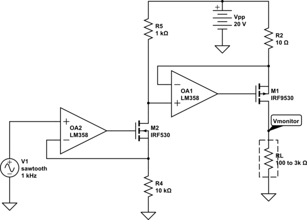
I'm designing a circuit for driving multiple loads (min. 16, up to 64) like the one shown below
schematic

simulate this circuit – Schematic created using CircuitLab

The input source is from a multi-channel DAC driven by an ATMega-like uC that can range from 0 to 5 V, and it should be able to generate a sawtooth with a minimum frequency of 1 kHz. As for the maximum frequency, this will be a trade-off between the resolution and speed of the scan. With this design, the circuit should be able to provide up to 50 mA to the load. The load resistance can vary from 100 to 3000 Ohm.

The problem is, I need to know accurately how much power is delivered to the load and I have a tight requirement of max 100 mW for each. For this reason, I'd like to introduce a monitor on the voltage using a multi-channel ADC and send it back to the uC. In this way, besides having a power monitor, I'd have a closed-loop feedback for better control. However, I'm afraid that placing the monitor in this way would cause a number of issues:

  1. (minor) Output resistance of the current source would be affected by the monitor (e.g. using a voltage divider before the ADC)
  2. (major) Need to share the SPI bus between the DAC and the ADC, lowering the maximum frequency I can obtain.

Before considering another uC, do you have any suggestion on how you would implement such functionality? Would you also consider the possibility to disable the monitoring for open-loop control?

\$\endgroup\$
10
  • 1
    \$\begingroup\$ I think you need to design your circuit to work firstly. There are several operational problems I can see. \$\endgroup\$
    – Andy aka
    Commented Jan 14, 2021 at 12:25
  • \$\begingroup\$ Sorry, I missed one piece of the schematic, I'll edit that. If even in that case it doesn't work, I'll ask you for more insight \$\endgroup\$ Commented Jan 14, 2021 at 12:29
  • \$\begingroup\$ I would concentrate on making this two questions then. Part (a) is how do I make a circuit that does what I want and, on another separate question, part (b) is your current question with the improved circuit agreed in part (a). Don't try and shoe-horn (a) and (b) into one question. \$\endgroup\$
    – Andy aka
    Commented Jan 14, 2021 at 12:31
  • \$\begingroup\$ Sorry, I thought that the schematic I drawn would have simplified the question, but I realized that it was not equivalent to the one I show now. \$\endgroup\$ Commented Jan 14, 2021 at 12:33
  • \$\begingroup\$ This circuit should work as expected. If that's not the case, I can't see where it could be my mistake. \$\endgroup\$ Commented Jan 14, 2021 at 12:35

1 Answer 1

1
\$\begingroup\$

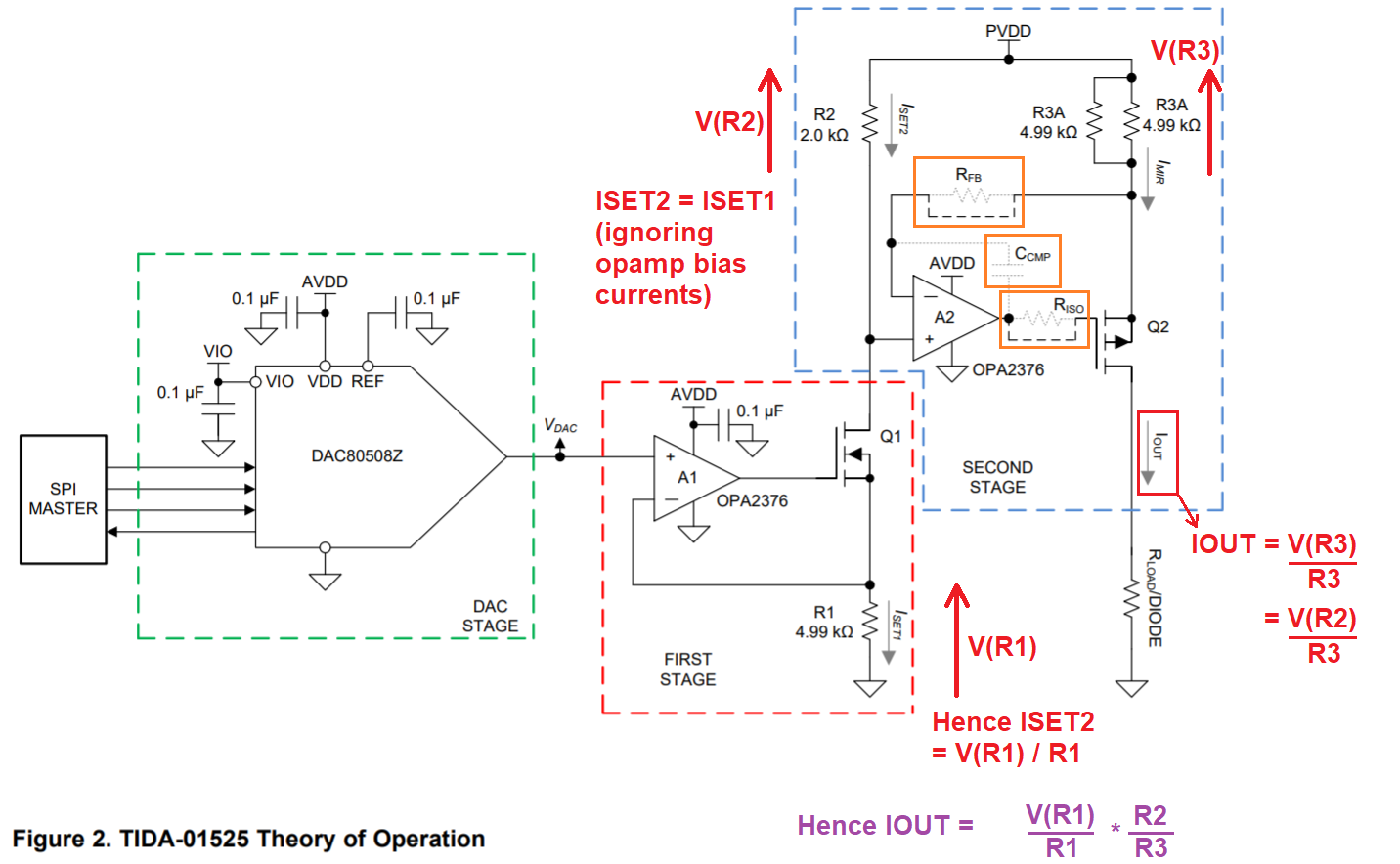
If you do use this type of schematic from TI it should work (on a more limited power supply): -

enter image description here

In the comments below the question I explained why the proposed circuit won't work (take note of op-amp type and the components in the orange boxes in my schematic). Those boxed components will certainly be needed if R3 is going to be as low as 10 Ω.

Also take note that the TI design uses an OPA2376 op-amp and this limits the power supply to no-more than 5.5 volts. You need to find a rail-to-rail op-amp that has decent spec and can operate from a 20 volt supply (as per the faulty diagram in the question).

I added a few notes and basically, if you monitor V(R1) and you have accurate resistors you can reliably predict load current: -

$$I_{OUT} = \dfrac{V(R_1)}{R_1}\times\dfrac{R_2}{R_3}$$

Use a high impedance voltage monitor circuit to measure this voltage. A 1 MΩ input impedance will degrade R1 to a 0.5% lower value for instance. I'd go for at least 10 MΩ input impedance for the monitor on R1 in my schematic.

For the output voltage monitor, keep with an input impedance of 10 MΩ or greater.

Need to share the SPI bus between the DAC and the ADC, lowering the maximum frequency I can obtain.

That's something that cannot be answered here.

Would you also consider the possibility to disable the monitoring for open-loop control?

That's up to you. Adding a few bells and whistles is always a good thing to do at an early stage rather than try and bodge in something later on.

It's almost imperative that you use a simulator to test this before committing to a PCB layout.

\$\endgroup\$
2
  • \$\begingroup\$ Hi, thanks for your reply, I'll definitely put up a simulation for this schematic and consider also the voltage monitor on R1. Before going deeper on this, just few notes: 1) on the schematic you show, extracted from the TI note, the R3 value should be 4.99 Ohm (two in parallel) and not 4.99k; they use the correct value later, I guess it's an error from their side. 2) the additional components placed in the orange boxes are not included in their final PCB layout. Is it because of their op-amp + fet selection and the lower operating voltage? \$\endgroup\$ Commented Jan 14, 2021 at 14:11
  • \$\begingroup\$ @ManuelReza I can't say why TI didn't add those components - maybe they found that in an earlier prototype they weren't needed for the op-amp used. Personally, I would add them so that at least you have coverage to fix things should the circuit burst into song as an oscillator. \$\endgroup\$
    – Andy aka
    Commented Jan 14, 2021 at 14:15

Your Answer

By clicking “Post Your Answer”, you agree to our terms of service and acknowledge you have read our privacy policy.

Not the answer you're looking for? Browse other questions tagged or ask your own question.