1
\$\begingroup\$

In many Texas Instruments datasheets (e.g. this one) there are two different stated values for current per output:

  1. Output drive, stated as 4 mA at \$V_{cc}=5 V \$, page 1.
  2. Continuous maximum current per output, stated as 25 mA, page 6.

My interpretation here is that if the device is operated at \$V_{cc}=5 V \$, TI guarantees that it can provide 4 mA per output. However, along with the second line it means that each output might also be able to provide \$4 mA < I_{output} < 25 mA \$ without damage, but the manufacturer doesn't recommend more than 4 mA at this supply voltage. Is this correct?

\$\endgroup\$
2
  • \$\begingroup\$ Notice also tables 7.5, 7.6 which guarantee the output voltage at 4mA (and 5.2mA but only if Vcc = 6V). Exceed 4mA only if you don't care what voltage you are supplying the next stage with! \$\endgroup\$
    – user16324
    Commented Feb 7, 2021 at 23:47
  • \$\begingroup\$ @BrianDrummond Thanks for the comment; to clarify, how are these output voltages measured? If a static CMOS gate drives another static CMOS gate then the steady-state output current is zero, so presumably the load is a resistive load of some kind, but then doesn't the output voltage depend on the value of that load (for a given current)? \$\endgroup\$
    – Halleff
    Commented Feb 8, 2021 at 1:06

2 Answers 2

7
\$\begingroup\$

On page one, the datasheet is telling you that the output can supply 4mA and still respect VOH(min). In other words, it can supply 4mA and still provide an output voltage that will be recognized as a logic level high by other IC's. It may be able to supply more than 4mA but the output voltage will sag. If you are not feeding the output to a logic device, but are instead using it to drive an LED at 5 or 8 mA, that sag may be acceptable to you. (Although I would look for a higher drive IC, personally, as this one is weak-ish for an LED).

On page six, you are looking at absolute maximum limits. It can supply 25mA without immediate damage (although damage may occur if you are at the absolute maximum for a long time). In general, you never design anything to be close to the absolute maximum for the IC in normal operation. This table, absolute maximums, is something you study so you can stay away from it. It is a "don't do this" table.

Absolute maximums tell you conditions that may cause permanent damage. No guarantee of correct behavior is implied.

You may also want to study tables 7.5, 7.6, and 7.7 to see how the guaranteed minimum value of VOH(min) varies with VCC and temperature range.

\$\endgroup\$
4
  • \$\begingroup\$ Thanks a lot for the answer. To make sure I understand, suppose we're operating the device at \$V_{cc} = 4.5 V\$. According to table 7.3, this means the minimum voltage the device can recognize as a high input (\$V_{IH}\$) is 3.15 V, so the device needs to be able to produce a minimum output high \$V_{OH} > 3.15 V\$. Then table 7.5 says that since \$V_{cc} = 4.5 V\$, if 4 mA is supplied to the output then the output is guaranteed to be at least 3.98 V, thus satisfying the minimum requirement with some margin. Is this correct? \$\endgroup\$
    – Halleff
    Commented Feb 8, 2021 at 0:54
  • \$\begingroup\$ I think generally yes, you get it. But different IC's may have different Vih and Voh. So the important thing is to make sure that the Voh of the driving device is compatible (higher than, in other words) with the Vih of the receiving device. And yes, there should be some margin. Without margin any little bit of noise could lead to incorrect states. There is a similar situation with Vol and Vil. \$\endgroup\$
    – user57037
    Commented Feb 8, 2021 at 1:20
  • \$\begingroup\$ Ok, thanks again. I think my last bit of confusion is how a certain output voltage for a certain output current can be guaranteed. Since (at least for CMOS gates), a driver provides 0 steady-state current to the next gate, where is this output current going? It doesn't seem to make sense for this to be output current during a switching transient since I don't think the concepts of input/output levels apply during the transients, only once things have settled. \$\endgroup\$
    – Halleff
    Commented Feb 8, 2021 at 1:25
  • \$\begingroup\$ Your confusion is reasonable. The output level is a DC level. Sometimes designers add pullups or pulldowns to logic outputs. Sometimes they may interface to old logic families that have non-zero input current. Sometimes they add an LED to an output so they can visually confirm its state. So the datasheet is just promising you, the designer, that as long as you manage to keep the DC load current under 4mA, they will keep the output voltage at the specified level. \$\endgroup\$
    – user57037
    Commented Feb 8, 2021 at 3:13
3
\$\begingroup\$

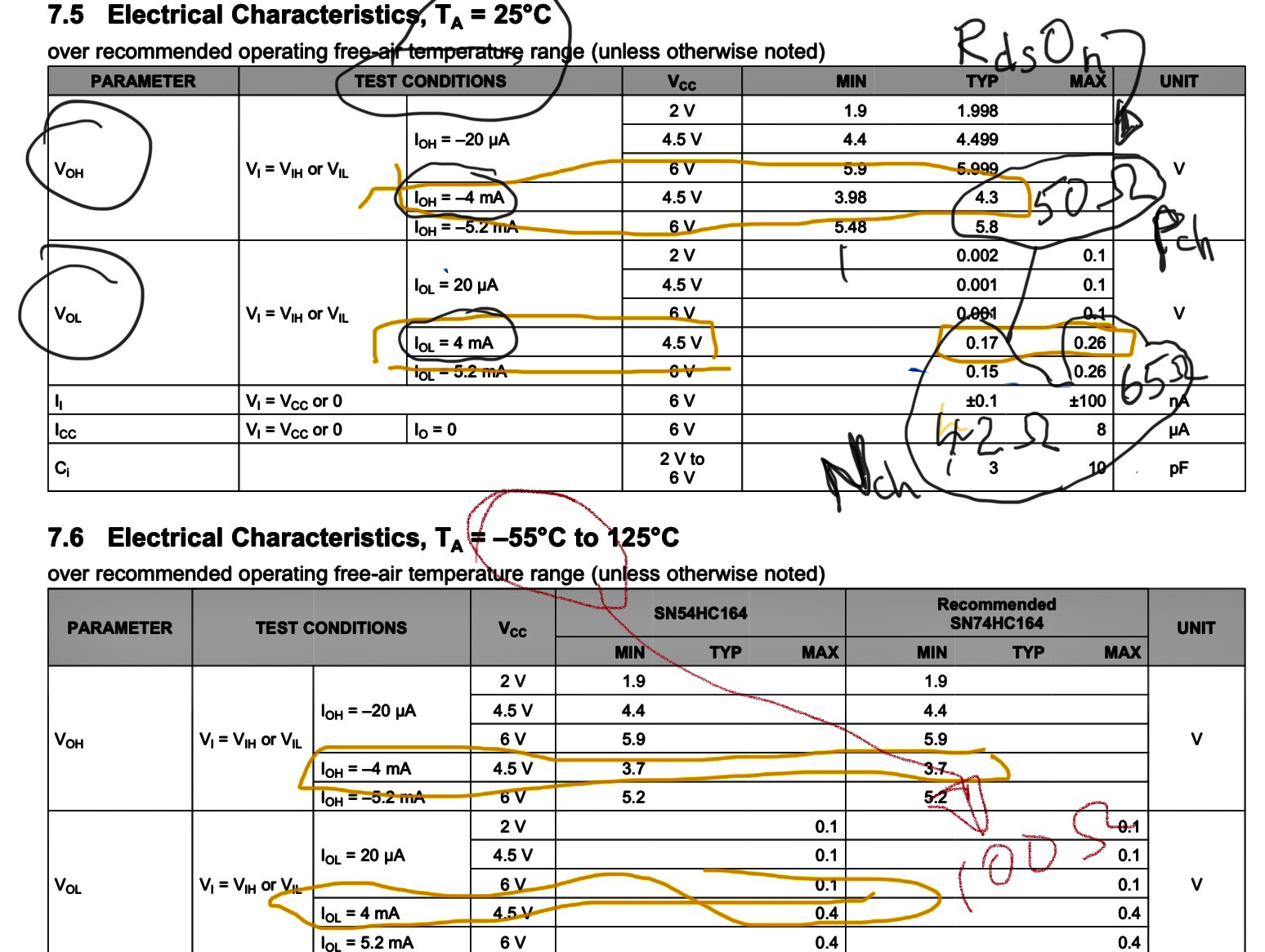
RdsOn is the FET switch analog parameter which limits risetime in a std load pF value and voltage drop or rise guarantee with somewhat standardized test currents. If you compute RdsOn for Vol/Iol and Voh at the specified Vdd you will understand how it affects risetime into a given load capacitance from the RC=tau value.

All logic devices are analog

In this case 4mA load applies to the worse case tolerance of -10% Vdd for a 5V supply, namely 4.5V. enter image description here

  • RdsOn rises with lower Vdd, lower temperatures
  • I usually call all 74HC family logic “50 ohm logic” at 5V but as you see there are tolerances on Vdd, batch tolerances and temperature tolerances.

Then I call 3.6V ARM or 74ALC family Cortex logic as 25 Ohm logic even though these are understood to affect risetime and voltage drop from each rail under a std. load current.

As stated in the absolute maximum 32 mA intended as a safety limit. I understand it is limited by a safe holding current before possible fusing of the gold wire bond to the substrate.

\$\endgroup\$
10
  • \$\begingroup\$ Thanks, this is helpful. I have a question about these tables: in this datasheet (and also for inverter datasheets like this one) under the "test conditions" column for like V_OH, they have the input as both V_IH and V_IL. How does it make sense to include both low and high inputs for the output high voltage, especially for an inverter? \$\endgroup\$
    – Halleff
    Commented Feb 8, 2021 at 3:48
  • \$\begingroup\$ The Louvre called, they're missing a Picasso :) \$\endgroup\$
    – po.pe
    Commented Feb 8, 2021 at 15:38
  • \$\begingroup\$ V_IH and V_IL are labels for logic levels so the only time it makes sense for both input and output to be at the same logic level for any inverter is during a transition time for T< t_pd . which may be confusing but essential they are saying the output impedance does not depending on the input state, It only matters if you assume the output is a valid logic level. So a defined load current infers the voltage drop across the switch in that state. Yes it's not obvious what they mean \$\endgroup\$
    – D.A.S.
    Commented Feb 8, 2021 at 16:18
  • \$\begingroup\$ :) funny @po.pe \$\endgroup\$
    – D.A.S.
    Commented Feb 8, 2021 at 16:25
  • \$\begingroup\$ Falstad's simulator is based on simple physics. The model for logic inverters is defined by the property of rise time only and Zout=0, but in datasheets is for a standard load pF and nominal RdsOn. Yet Falstad's logic is if you want to simulate the analog properties better, add a series R to the output drivers ( same with Op Amps like add 200 Ohms the typical BJT open loop Zout) But to make the simulator fast in realtime, this assumption makes it work fast and is approximate but valid for finding races or making loops oscillators but invalid if you don't add RdsOn tinyurl.com/y2roy446 \$\endgroup\$
    – D.A.S.
    Commented Feb 8, 2021 at 16:43

Your Answer

By clicking “Post Your Answer”, you agree to our terms of service and acknowledge you have read our privacy policy.

Not the answer you're looking for? Browse other questions tagged or ask your own question.