-2
\$\begingroup\$

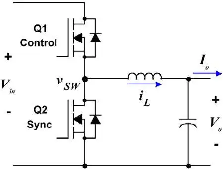
I want to make a buck converter with bidirectional GaN FETs, so each switch is made up of two back-to-back GaNs:

enter image description here

The problem that I encountered is that if I have a deadtime (DT) higher than 0 ns between the two switches, I end up having huge spikes of voltage at Vsw (in the order of kV) but the expected output looks fine. If the dead time is 0 then the waveforms look as they should.

Also, if I build the same circuit but instead of having bidirectional switches, I use normal switches, I have no problem at Vsw, no matter the duration of DT.

I don't understand why I have this behavior in simulation and how I can overcome it.

\$\endgroup\$
5
  • 1
    \$\begingroup\$ Do you understand how inductance works when current flows through it and it is disconnected from circuit? Just checking how far back in the basics we must go in the explanation. \$\endgroup\$
    – Justme
    Commented Oct 8, 2021 at 12:02
  • 3
    \$\begingroup\$ "back-to-back GaNs" Why? \$\endgroup\$
    – winny
    Commented Oct 8, 2021 at 12:06
  • 1
    \$\begingroup\$ This video by Dave from the EEVBlog explains what happens when you apply a voltage to an inductor (relay) and then suddenly break the connection: back EMF: youtube.com/watch?v=hReCPMIcLHg Sure, Dave powers a relay but that's also an inductor so the same thing happens in your circuit. \$\endgroup\$ Commented Oct 8, 2021 at 12:15
  • \$\begingroup\$ Using bidirectional MOSFETs is missing a trick in my book. Please explain why this is necessary (the root cause of the back emf of course). \$\endgroup\$
    – Andy aka
    Commented Oct 8, 2021 at 12:22
  • \$\begingroup\$ You need to read more about the fundamental basics of buck converters before building one, let alone one with your own modifications. You skipped a few steps. Do you even know why Q2 is there? Or why any component (transistor or not) is even in Q2's position in all buck converters? \$\endgroup\$
    – DKNguyen
    Commented Oct 8, 2021 at 13:25

1 Answer 1

1
\$\begingroup\$

In regular MOSFETs, which can conduct in reverse, the inductor current can pass through one of the MOSFETs during the deadtime.

If you use bidirectionally blocking switches, then the inductor current has to collapse immediately after turn of, which induces a huge voltage at the switch node.

An obvious remedy is the use of regular MOSFETs (or GaN FETs). Another possible remedy is to add a capacitor to Ground to the switch node. But this will eat a lot of current instead (but stabilize voltage). A R-C snubber will be somewhere between a lot of current and a lot of voltage spiking...

\$\endgroup\$
1
  • \$\begingroup\$ OP is in a bad spot here. RC from vsw to ground or MOV to clamp the peak voltage somewhat?? \$\endgroup\$
    – winny
    Commented Oct 8, 2021 at 12:07

Not the answer you're looking for? Browse other questions tagged or ask your own question.