0
\$\begingroup\$

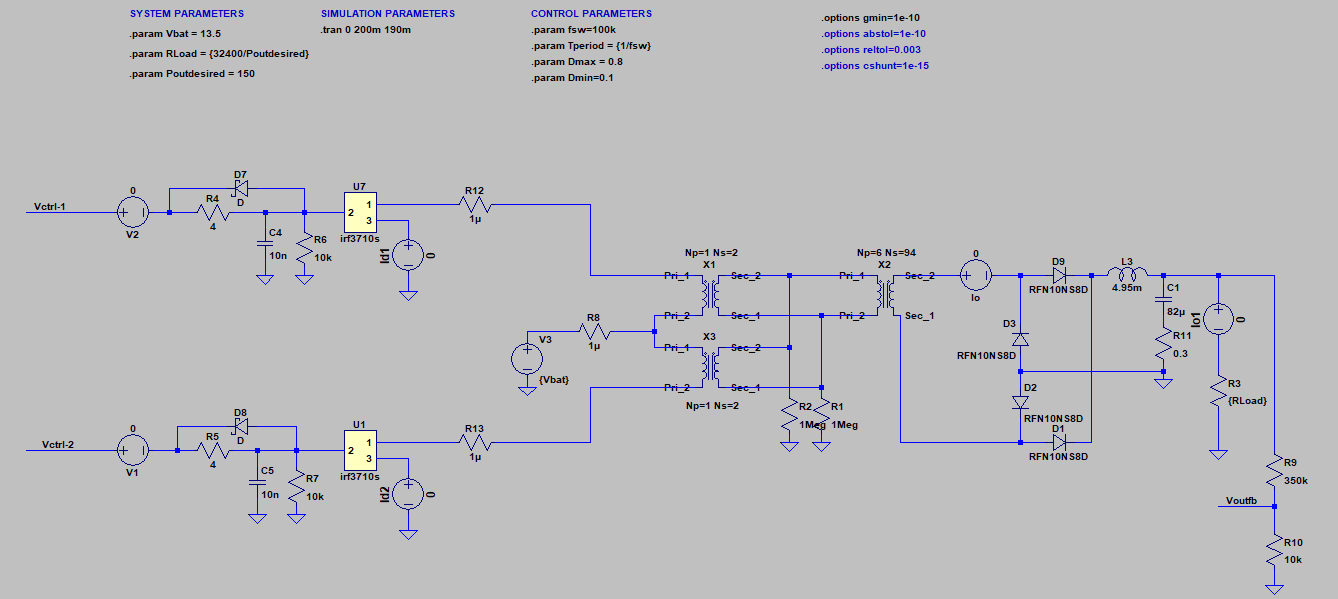
I am simulating a 150W push-pull converter in LTSpice as shown below:Push Pull simulation
I'm viewing the waveforms after 200mS which I believe is giving stabilized readings. I'm seeing huge current spikes on the drains of each FET:FET current spike
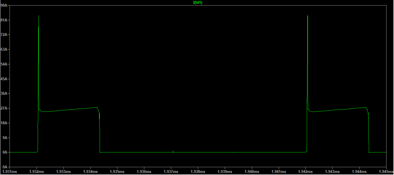
These spikes are symmetrical on both FETs, but each FET has no voltage ringing at all; the drains look perfect in terms of voltage. The current after the spike is about what I would expect from the system currently.

I'm not sure where this spike is originating from: the inductor is high enough that the system is in CCM, the output capacitor is not spiking, and the Rload is consistent and purely resistive. The diodes are an LTSpice component with an average current of 10A and a Vbr of 800V, so they shouldn't be breaking down.

At this point in the simulation the waveforms are being looked at the duty cycle is a consistent 22.8%.

Any help is appreciated.

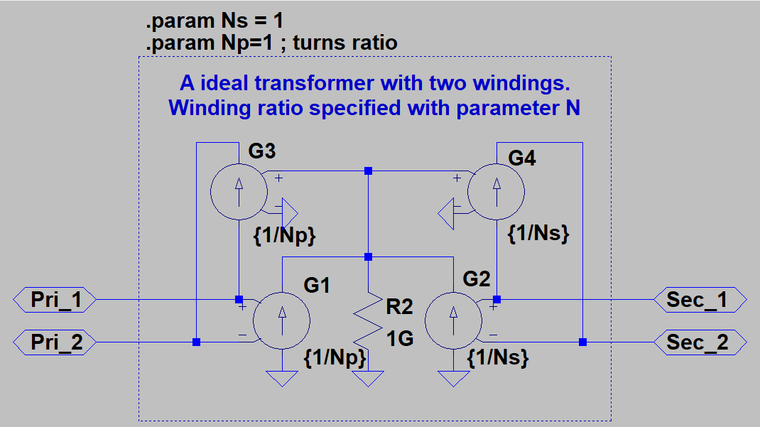
EDIT The duty cycle control is two control signals with a minimum of 20% dead time, or about 2uS. Here is the subcircuit model for the transformer. Each coil pair is made of this model, there are three total to simulate the full transformer operation.transformer subcircuit
\$\endgroup\$
3
  • 1
    \$\begingroup\$ Is there a dead-time between the two gate-drive signals? \$\endgroup\$ Commented Jul 23, 2021 at 3:09
  • 1
    \$\begingroup\$ I don't know if it matters for the circuit...but although D7 and D8 are drawn with Schottky symbols, they are calling the model D which is a silicon PN diode with all default parameters. If you need a Schottky there, you should pick one from the internal part list which suits your needs. \$\endgroup\$
    – Ste Kulov
    Commented Jul 23, 2021 at 4:14
  • \$\begingroup\$ I don't think the diodes are an issue since the spike happens at FET turn on and not turn off. There is considerable dead time between each turn on. \$\endgroup\$
    – pbandjazz
    Commented Jul 23, 2021 at 18:15

2 Answers 2

2
\$\begingroup\$

Likely you don't have any non-overlap in the gate drive (i.e. you need a point where VGS is low for BOTH FETs just before toggling states).

Another possibility (less likely) is that the gate drive is not strong enough -- as the drain V rises, it capacitively couples to the gate of the 'off' FET and turns it on again.

In either case, if the transformers are 'ideal' (i.e. no leakage inductance), the FETs will appear to see a short circuit and you will get spikes of current.

\$\endgroup\$
4
  • \$\begingroup\$ Plus the MOSFETs take a while to have the Vds decrease while the Vgs dropped to zero (similar problem). It could be mitigated with slow turn on and fast turn off. \$\endgroup\$ Commented Jul 23, 2021 at 5:25
  • \$\begingroup\$ There is considerable dead time between each turn on. The transformers are ideal elements, but why would the FETs see a short circuit, wouldn't it see the output stage as though it were connected to the FETs? \$\endgroup\$
    – pbandjazz
    Commented Jul 23, 2021 at 18:18
  • \$\begingroup\$ @pbandjazz Can you show us the subcircuit you are using for the transformers? \$\endgroup\$
    – Ste Kulov
    Commented Jul 24, 2021 at 3:05
  • \$\begingroup\$ OP has been edited. \$\endgroup\$
    – pbandjazz
    Commented Jul 28, 2021 at 21:39
0
\$\begingroup\$

I'm not sure where this spike is originating from:

Check all nodes to the FET, the current should add to zero. If it's not then the model is creating currents (I've seen this before from bad models with improper ideal sources 'creating energy' in what should be a passive device). Also have a look at the FET's spice model and see if it makes sense.

Another thing is the model should probably have some parasitic trance resistance and inductance. Estimate what a PCB trace would be (or use something like 10mΩ and 10nH).

\$\endgroup\$

Your Answer

By clicking “Post Your Answer”, you agree to our terms of service and acknowledge you have read our privacy policy.

Not the answer you're looking for? Browse other questions tagged or ask your own question.