I have very limited PCB design experience. I've been using this program called Fritzing (it... has its pros and cons). Something I noticed is that when I do a ground fill with this software, it leaves copperless borders around ground pins except for traces I manually draw.
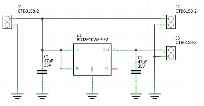
For example, here is a rough draft of a power supply board I'm trying to make. The circuit, for reference, is:
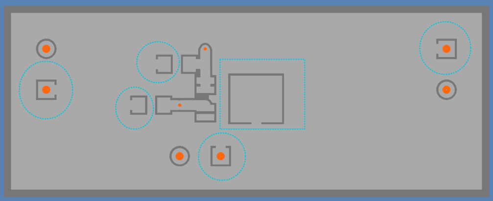
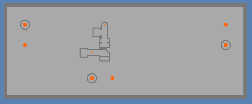
It's just a linear regulator, some capacitors, and some terminals. Now, take a corresponding PCB layout. This is a rendering of the copper mask (light gray) on the ground layer:
I've drawn blue dotted lines around the ground pads.
As you can see, there are borders around the ground pins, with only one edge of each pin connected. Most notably there's very minimal copper between the regulators heat sink fin and the rest of the copper fill.
I suspect that this is not a good idea. My gut tells me there should be copper all around those pins, if only for heat management, e.g. something like:
So, my question is: Is my suspicion correct? Should those border areas around the pins also be filled with copper?
Note: The above PCB is my first draft of this design; I'm aware that it might need improvements; e.g. routing practices, via and trace sizes, capacitor selection and placement, etc. But, no spoilers please! 😁 I'm saving that for its own question after I do a little research. For this question, I'm just wondering about those ground fill pin borders in general.


