2
\$\begingroup\$

Sorry for the naive question! I want it to be specific enough to be answerable, but I'm not sure how to find the answer to my actual question, so I'm asking it here. Another way to put it might be "why are circuit boards becoming more aesthetically pleasing?"

I've included some comparisons of older and newer products below, but the general trends I've noticed are:

  • Smoother edges.
  • More matte/lighter solder masks.
  • Less-visible solder traces.
  • Rounded corners.
  • Solder masks that appear to seamlessly blend with through holes.
  • ICs with perfectly-crisp edges.

What I'm wondering is that has caused these changes. All three examples I included below are from newer companies, so is this just a case of them improving their design and manufacturing processes? Has some new manufacturing technology supplanted an old one? Have manufacturers changed their processes across the industry in some way?

Basically: Have these companies just become better at designing boards, or has the industry made some broad improvement to manufacturing processes (at least in these examples)? What is causing the overall visual change?

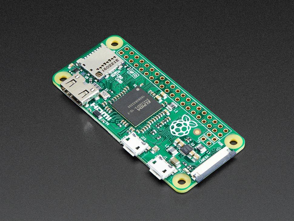
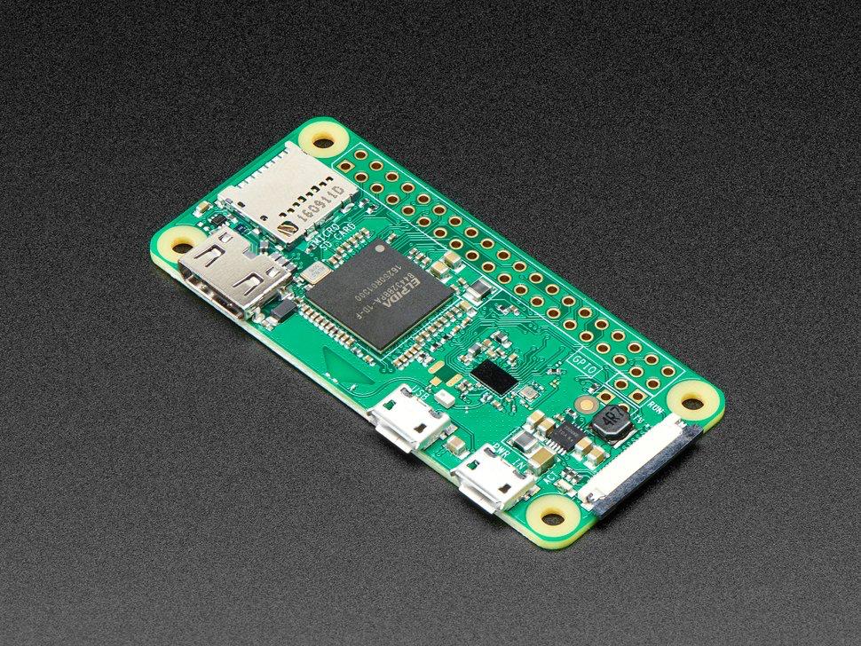
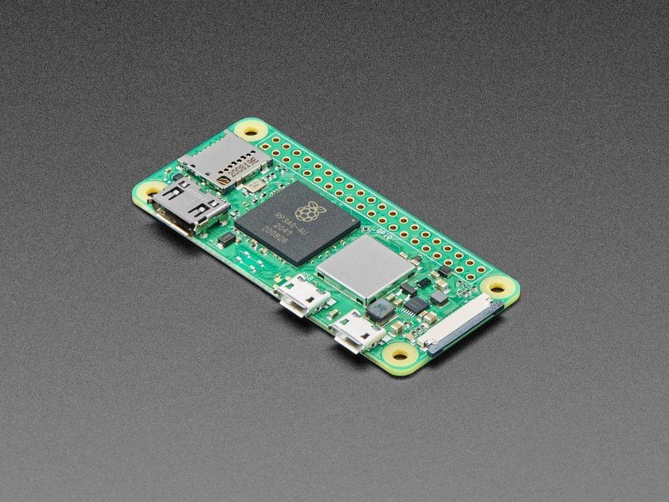
Original Raspberry Pi Zero Raspberry Pi Zero W New Raspberry Pi Zero W 2
Original Raspberry Pi Zero Raspberry Pi Zero W Raspberry Pi Zero W 2
Dark traces, dark solder mask, very rough edges. Clearly-visible traces, darker solder mask, GPIO holes that seem to have an edge to them. Lighter solder mask, GPIO holes seem to be flush with the mask, all chips have very crisp edges. The difference is much more visible in person.
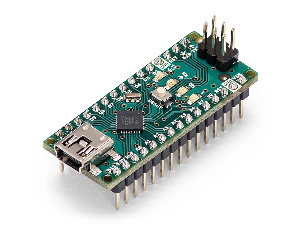
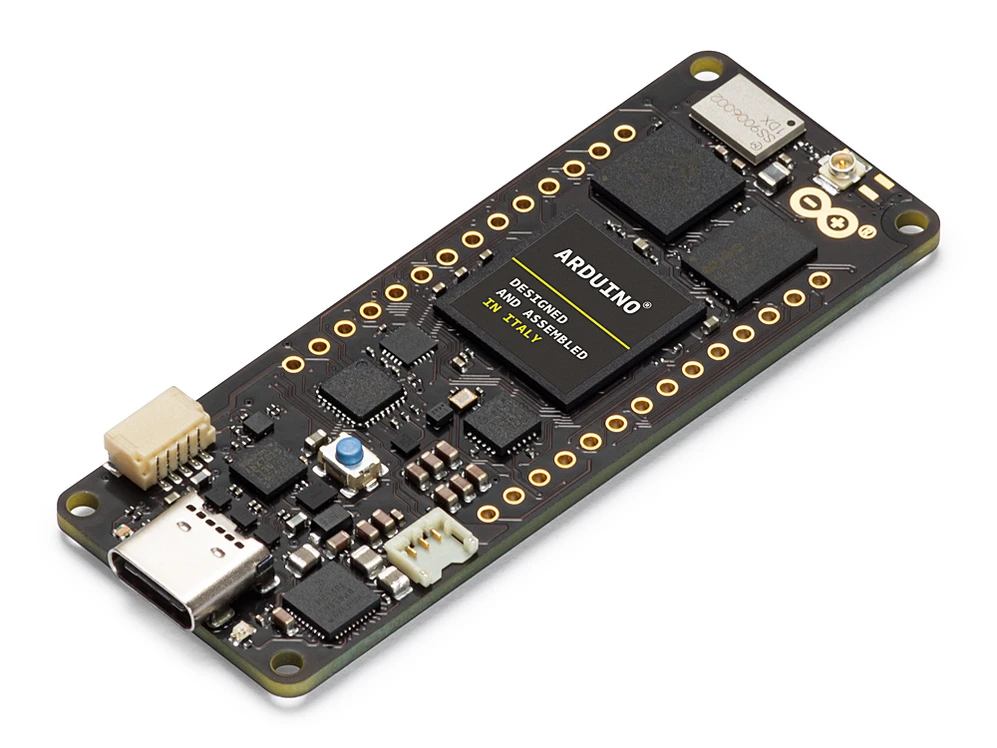
Arduino Nano Portenta H7
Rough edges, visible traces, sharp corners. Smoothly-finished edges, rounded corners, crisp solder mask border around the through-holes.
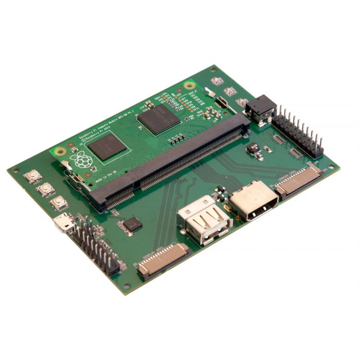
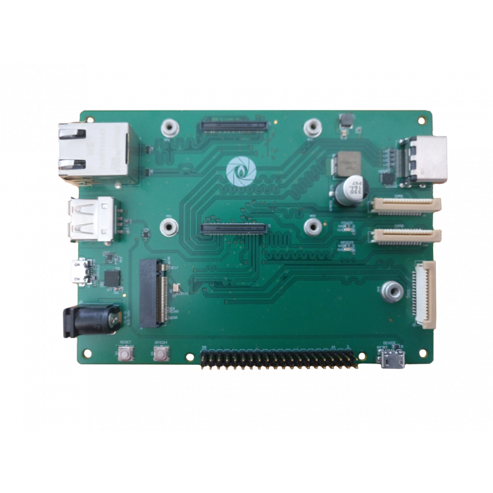
Gumstix Pi Compute Dev Board Gumstix Raspberry Pi CM4 Development Board
Sharp corners, unfinished edge, darker solder mask. Rounded corners, mounting holes look "firmer", lighter solder mask.
\$\endgroup\$
5
  • 1
    \$\begingroup\$ I don't think this can be answered very definitively. My own experience in the PCB industry suggests all of these changes can be driven simply by 1) more people involved in and gaining better access to PCB design; 2) fabricators improving processes and lowering costs on more advanced features; 3) an increasing number of products include PCBs for connectivity and convenience. I don't think there's a sudden change or increase in quality but rather a continuous trend that if plotted on a timeline would probably be somewhat exponential. \$\endgroup\$
    – JYelton
    Commented Dec 7, 2021 at 18:59
  • 1
    \$\begingroup\$ ""why are circuit boards becoming more aesthetically pleasing?" - whether they have is a matter of opinion. I like traces that are clearly visible. I like dark solder masks. I hate rounded corners! 'ICs with perfectly-crisp edges' is not a PCB feature, but I hate those sharp edged BGA packages! (and I hate BGA in general - for obvious reasons). \$\endgroup\$ Commented Dec 7, 2021 at 19:11
  • \$\begingroup\$ @JYelton I'm guessing it might be largely (1). Basically, I'm wondering if I'm just imagining a pattern in otherwise gradual improvements, or if there's been some common factor like a major manufacturer of substrates/masks changing their process, for example. I wouldn't be surprised if I've just picked up on an RPI-driven trend. They had products with a consistent design for years, so it could be as simple as 1) RPi releases a batch of products with new form factors and an improved design language -> 2) the adjacent IoT/SBC/prototyping space follows suit. \$\endgroup\$ Commented Dec 7, 2021 at 19:25
  • \$\begingroup\$ @BruceAbbott I guess a better way to put it would be "why do the newer products from many different companies seem to have shifted to a more intentional visual aesthetic all around the same time?" Or "why do the products on the right look much more likely to have been designed by Apple than the products on the left?" \$\endgroup\$ Commented Dec 7, 2021 at 19:32
  • \$\begingroup\$ Most of it is driven by the technology, but there is definitely an esthetic element involved in your examples. These boards are often used 'bare' with their advanced circuitry on show, and users want them to look 'pretty'. But I look at these boards and just see trouble - tiny components, delicate connectors, hair thin traces, sensitive low voltage BGA ICs that are impossible to replace with normal equipment. Better to cover it up in an ESD safe case as soon as possible! \$\endgroup\$ Commented Dec 7, 2021 at 20:18

0