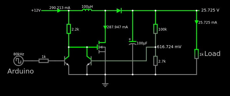
This seemed to work quite well and noise was kept to a minimum. Best of all, it's super simple!
It doesn't really work the way you desire. A switching regulator needs to:
Actually switch
The mosfet is operating in the linear mode - not as a switch. That's thanks to the feedback transistor.
Provide sufficient gate drive
Power mosfets are large devices, with gate capacitances measured in nanofarads. The time constant of the 2.2k pull up with 1nF is a couple microseconds - that's very slow switching, given that the period is just 12.5μs. Power mosfet gate needs to be driven with a push-pull or totem pole circuit.
Control the inductor current
The inductor current neither returns to zero on each cycle, nor is it limited in any way. Even if there was switching, the inductor current would be liable to run away.
Is this boost converter feedback technique a good idea?
Sorta-kinda. Not as shown, but indeed negative voltage feedback would have this sort of a "shape" when looked from a high level. The actual circuit you propose doesn't work.
Is the particular topology you chose a good fit for the application? Not quite. One-inductor boost converters with high step-up ratios run at high inductor currents, and are not very efficient due to conduction losses in the inductor, mosfet channel, diode, etc. The high-voltage rated mosfets have relatively high channel resistance.
A flyback converter with a simple, very cheap controller chip, like MC34063, would be much easier to implement - even if you were to wind your own transformer for it. You can buy off-the-shelf 1:1:1 inductors that can be set up for 1:2 step-up function - even that would be a win in this circuit. It'd halve the inductor and switch current.
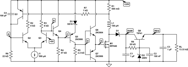
At minimum, the inductor current has to be controlled, given the high duty cycle and the tendency for inductor current runaway in such circumstances. The circuit below does that.

simulate this circuit – Schematic created using CircuitLab
Q1 is the inductor current limit detector. R6 generates a ramp over R4. The ramp is compared to a reference voltage by the differential pair Q2-Q3. Q4 and Q5 provide additional gain. The Q6-Q7 follower drives the gate of the mosfet M1. Q8 provides linear post-regulation. The maximum RAW voltage is limited by the losses in the circuit, as well as duty cycle limitations inherent in its design.
While this is not a ready-to-use circuit, it could be one of many starting points in investigating a discrete solution (without ICs). It at least pretends to work in the simulator :)
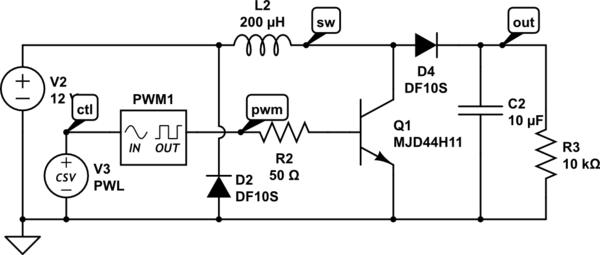
The first potential improvement, shown below, would be to use the mosfet's channel resistance Rds(on) as a current sensor. Q1 uses the gate control signal G to turn off the current feedback when the switch is off. Differential pair Q2-Q3 is the switch current limit comparator. R7-R8 generate the current cut-off reference voltage from the stabilized 15V generated by R4. C2-R2 is the ramp generator. The linear post-regulator is not shown.

simulate this circuit
The switch turn-on timing is still a based on a ramp with timing determined by C2-R2.
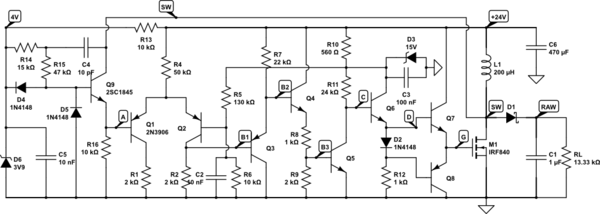
Instead, we can be using the collapsing switch voltage to turn the switch back on. The circuit below uses a high voltage transistor Q9 as a switch voltage clamp. Switch voltages below about 4V are presented on the feedback input A into the differential pair Q1-Q2. R6-R5-C2 set the peak inductor current. Decrease R5 to increase the current, and vice-versa. Q3-Q4-Q5-Q6 are gain stages implementing a comparator. Circuitry around Q5 could use some improvement. Q7-Q8 are the gate driver.
The circuit oscillates at about 80kHz, as determined by the value of L1. The frequency is variable around this nominal value and depends on the output voltage.
The raw output voltage is limited by losses and peak inductor current. Adjusting the inductor current will set the raw output voltage level. Then a linear post-regulator is needed to remove ripple.
C1 must not be increased since it is initially charged via L1, and larger values will develop excessive inductor current. This initial transient starts up the oscillation as well.

simulate this circuit
The circuit self-oscillates and implements current-mode control. The switch is turned on when the inductor current reaches zero, and is turned off when the inductor current reaches the peak value (preset by R6-R7 ratio).

