0
\$\begingroup\$

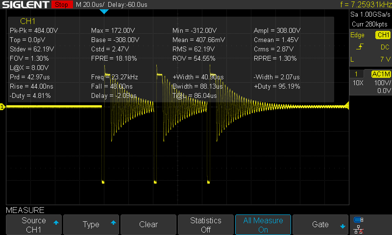
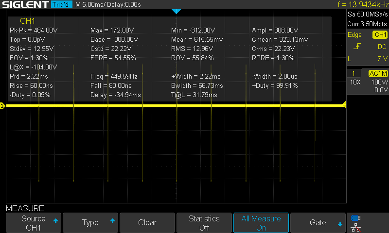
In the process of attempting to modify the output voltage of an existing SMPS (see sketched circuit), I've come across unexpected waveforms of the step-down transformer (see two snapshots of primary coil, two time bases). I was expecting a square wave (instead of a "fading-ringing" occurring 3 times in sequence) oscillating at a frequency specified by the PWM controller (DP2281 with Fixed Switching Frequency of 65kHz). I was hoping someone could explain what's going on.

Thanks

P.S. This post is to help me progress with a previous post seeking help to modify the output voltage of a SMPS.

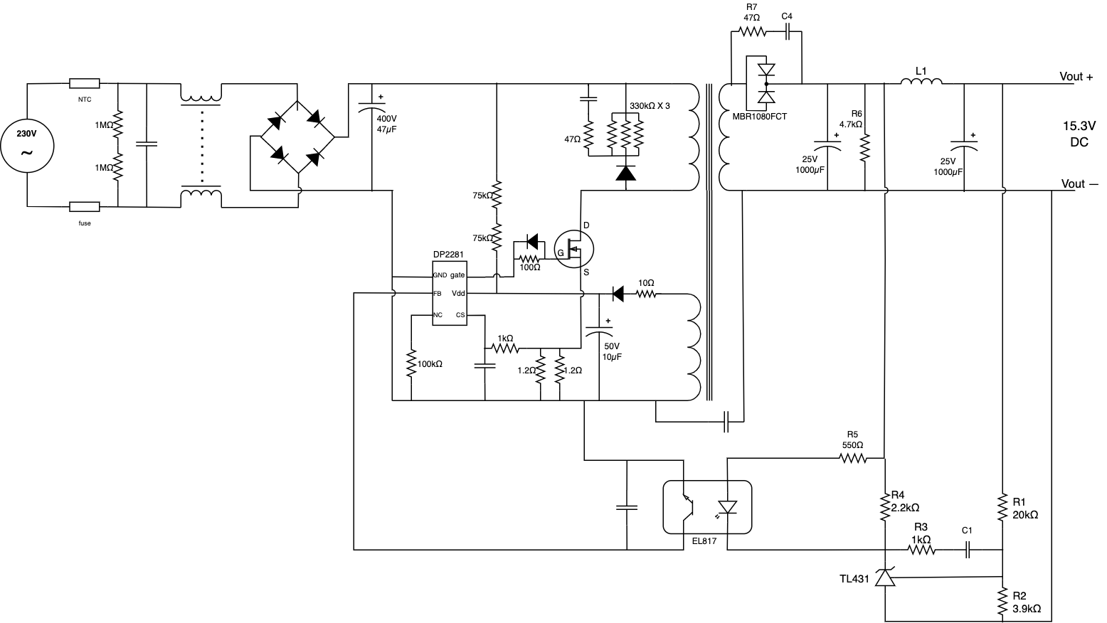
SMPS Circuit diagram SMPS Circuit diagram

Primary waveform in 20 microseconds time base Primary waveform in 20 microseconds time base

Primary waveform in 5 milliseconds time base Primary waveform in 5 milliseconds time base

\$\endgroup\$
5
  • 1
    \$\begingroup\$ Looks like burst mode? What did you change? What do you hope to achieve that the former SMPS didn't have? \$\endgroup\$ Commented Mar 18, 2022 at 17:52
  • 2
    \$\begingroup\$ Looks pretty normal to me. Which part of the waveform needs explaining? \$\endgroup\$
    – Justme
    Commented Mar 18, 2022 at 18:12
  • \$\begingroup\$ No layout info, no BOM , no part values with DCR, ESR, no DC measurements, no photos, Question seriously lacks info. What part did you not understand about Extended Burst Mode control in datasheet? \$\endgroup\$
    – D.A.S.
    Commented Mar 18, 2022 at 18:14
  • 2
    \$\begingroup\$ Looks normal. DCM and burst mode? \$\endgroup\$
    – winny
    Commented Mar 18, 2022 at 18:41
  • \$\begingroup\$ I was hoping to reduce the output voltage from 15.3V to 5V. I've experimented a little with changing R1 & R2 so that they are equal in value, but that only brought the output to approx 9V. I am rusty with diagnosing circuits. The waveform I shared was not what I expected, so I first wanted to understand what I'm seeing. Regarding the BOM, the circuit diagram shows all the components, however some did not have values written on them (e.g. on surface capacitors) so their values do not show on the diagram. What measurements would be useful? I'll provide those. \$\endgroup\$
    – alonjr
    Commented Mar 18, 2022 at 18:53

1 Answer 1

3
\$\begingroup\$

I was expecting a square wave (instead of a "fading-ringing" occurring 3 times in sequence)

According to the data sheet of the DP2281, it's a flyback converter controller and, what you see is pretty much what all flyback converters produce regarding the waveforms.

The ringing is the leakage inductance of the transformer primary trying to get rid of the unused (and unusable) energy by dumping it into both the snubber and the power MOSFET's parasitic capacitance. Pretty typical I'd say.

So, that's the "fading-ringing" you see. Regarding only seeing three pulses then a bigger gap to another bunch of pulses (not captured on your o-scope), that's because the loading on the secondary circuit is quite light and the controller is going into burst mode having achieved its primary objective of producing the correct DC voltage on the secondary DC output.

I was hoping someone could explain what's going on.

Hopefully that's sorted now.

\$\endgroup\$
1
  • \$\begingroup\$ Very true, the output/load resistor used is quite big so its a light load condition, and as per datasheet the IC goes to burst mode with a base frequency of 22kHz. \$\endgroup\$ Commented Mar 19, 2022 at 5:02

Your Answer

By clicking “Post Your Answer”, you agree to our terms of service and acknowledge you have read our privacy policy.

Not the answer you're looking for? Browse other questions tagged or ask your own question.