1
\$\begingroup\$

I am a student and I want to design a PCB. I am using Altium Designer 22.

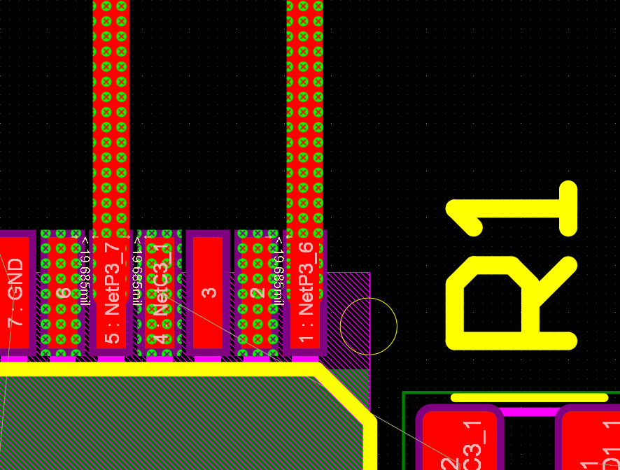
I selected 0.5 mm for the clearance constraint rule, but I got an error. If I select 0.3 mm I still get the same error. How can I solve this?

The IC in the picture is an FT232RL but I get the same error with a MicroUSB type-B connector.

like this

Error message: error message

\$\endgroup\$
1
  • \$\begingroup\$ I would recommend using the same units for rules and the PCB (F11 for properties, then metric) \$\endgroup\$
    – raaymaan
    Commented Apr 9, 2022 at 12:09

1 Answer 1

1
\$\begingroup\$

Set your rules correctly (track pad clearance, there are many rule settings) and use a narrower trace width- similar to pad width. You may have to adjust the track width rule to allow the narrower width.

Eg (this is a relatively fine multilayer board, your numbers will likely vary).

enter image description here

enter image description here

Note that the above rules are default, you can define different rules where necessary Eg. This particular board has 4 sets of rules for each of width and clearances, so around 400 rules for minimum electrical clearances alone. Fortunately you don't usually have to enter each one individually.

enter image description here

You can enter the rules in whichever system (metric vs. Imperial) you want by entering the unit after the number if it is different from the current display, to toggle display use the q key shortcut.

\$\endgroup\$

Your Answer

By clicking “Post Your Answer”, you agree to our terms of service and acknowledge you have read our privacy policy.

Not the answer you're looking for? Browse other questions tagged or ask your own question.