2
\$\begingroup\$

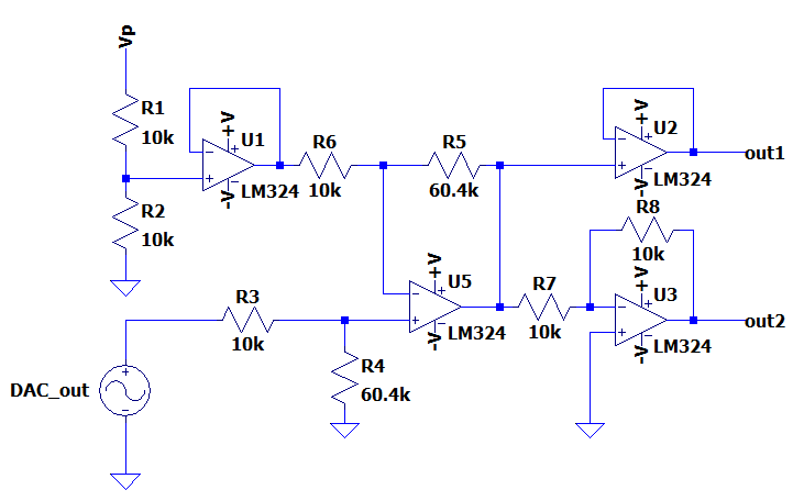
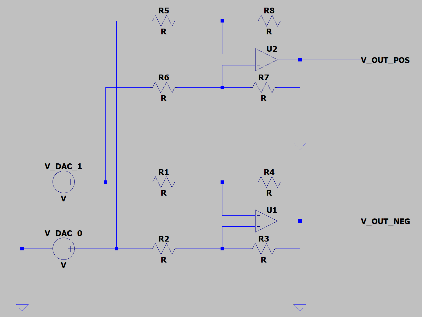
By using the following single LM324 circuit, I create amplified bipolar outputs from a 16-bit 0-3.3V DAC output as follows:

enter image description here

My aim is to minimize extra DC error due to the above LM324 circuit especially not to increase the DNL at the final output. Now for Vp I guess I can use a precision 3.3V voltage reference(?). But for the rest I'm not experienced enough to proceed.

How important in this case the supply/rail voltage stability? And how can we quatify the drift due to LM324?

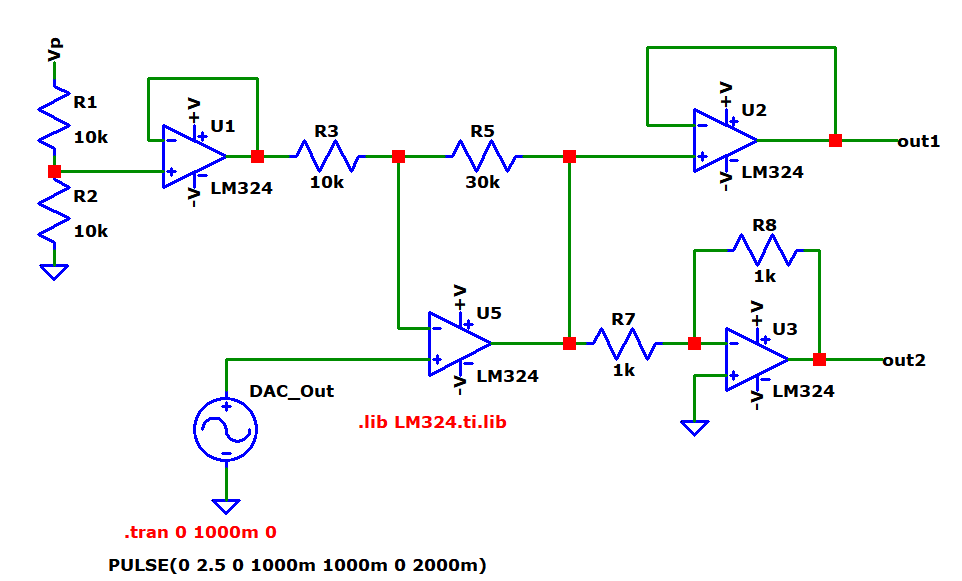
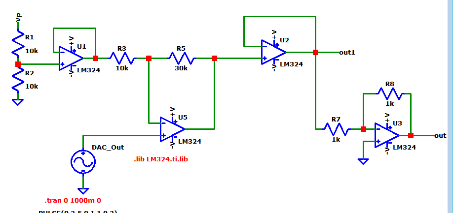
edit for an answer:

enter image description here

enter image description here

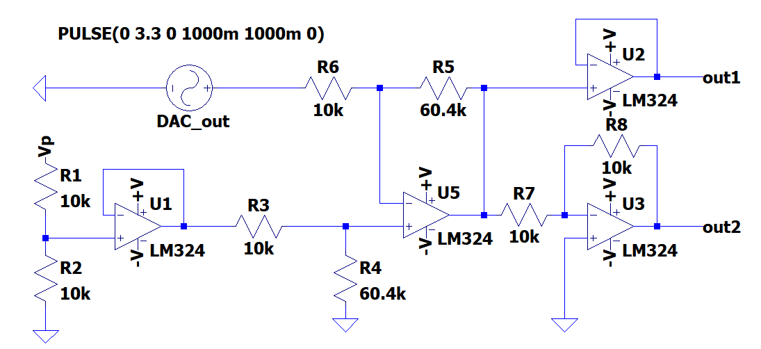
edit:

enter image description here

\$\endgroup\$
5
  • \$\begingroup\$ NB: I should use rail to rail (input and output) opamp for this application, something as TLV9104 well protected against EMI. \$\endgroup\$
    – Antonio51
    Commented Apr 19, 2022 at 11:15
  • \$\begingroup\$ At a quick glance you've got op amps that don't do anything. You can replace U1,R1,R2,R6 with 20K to Vp and 20k to ground. Remove U2 and get out1 from U5. \$\endgroup\$
    – stretch
    Commented Apr 19, 2022 at 14:46
  • 1
    \$\begingroup\$ @stretch out1 and out2 will go to a diff input of a device. U2 is buffer. Dont you think out1 and out2 will be unbalanced(different output impedances) if U2 is removed? Then more common mode voltage will appear as differential noise. (?) \$\endgroup\$
    – GNZ
    Commented Apr 19, 2022 at 17:06
  • \$\begingroup\$ @GNZ The imbalance would be small compared to the input offset errors, for a typical op amp. We don't know how much accuracy is needed or how much of a load out1 and out2 will see.. The 16 bit DAC has an LSB in the 10s of microvolts. The LM324 has input offset errors in single digit millivolts. The main problem, though, is that it can't sink much current, so U5's output can't go negative beyond about -200 mv. \$\endgroup\$
    – stretch
    Commented Apr 20, 2022 at 22:30
  • \$\begingroup\$ @stretch "U5's output can't go negative beyond about -200 mv." Supply is dual and U5 can go way below -200mV. I already implemented this circuit. Imbalance is important for CM voltages to turn into diff noise. \$\endgroup\$
    – GNZ
    Commented Apr 20, 2022 at 23:30

2 Answers 2

2
\$\begingroup\$

You should use the same reference for Vp as is used for the DAC, and it should be low noise and stable, preferably not a digital supply voltage. If you have to use a DAC that has no option other than to use the supply voltage as a reference, you can create a dedicated supply voltage just for the DAC and Vp.

DC nonlinearity is not greatly affected by your circuit, though you might want to switch up the inputs on your differential amplifier (DAC goes to the inverting input) since it has relatively high gain. That will essentially eliminate common-mode voltage rejection errors. Of course a precision op-amp would tend to yield better results all told.

Crossover distortion is quite noticeable for AC signals on the LM324 type output stage at frequencies as low as tens of Hz.

\$\endgroup\$
6
  • \$\begingroup\$ Than you for the answer. Regarding: "switch up the inputs on your differential amplifier (DAC goes to the inverting input)" Is that possible for you to add schematic to your answer? I tried myself and messed it up in simulation. I guess making some mistake. I would be very glad if you could show modified version(DAC going to inverting input case). \$\endgroup\$
    – GNZ
    Commented Apr 19, 2022 at 20:23
  • \$\begingroup\$ I edited and added your suggestion in my question: i.sstatic.net/0i6Bu.png Was that what you have meant? \$\endgroup\$
    – GNZ
    Commented Apr 20, 2022 at 0:12
  • \$\begingroup\$ Or this one is better? i.sstatic.net/08Ys3.png \$\endgroup\$
    – GNZ
    Commented Apr 20, 2022 at 0:25
  • \$\begingroup\$ I mean switch the output of U1 and DAC out connections. That reverses the outputs so out1 acts like out2 and vice versa. \$\endgroup\$ Commented Apr 20, 2022 at 2:46
  • \$\begingroup\$ Just swapped them like here: i.sstatic.net/Eh1DB.png This time correct right? Also why does this better for CM rejection? Thanks \$\endgroup\$
    – GNZ
    Commented Apr 20, 2022 at 17:11
1
\$\begingroup\$

The challenge with this circuit (as you've already alluded to) is that the differential output will be zero when the DAC is at some intermediate point. Your op-amps use a negative supply, but your DAC does not. Your voltage reference (Vp/2) and DAC output may drift, so you may not be able to reliably represent small differential voltages at the output.

A DAC designer could use feedback techniques WITHIN the DAC itself to ensure this value is always aligned to some ground reference, but I'm guessing you don't have that liberty.

Can you use two DACs? If so, the easiest solution that comes to mind would be to use DAC1 for when your signal is greater than 0 and use DAC0 when your signal is less than zero. Otherwise, each DAC outputs 0[V]:

1

Small bonus: this effectively creates an 17-bit DAC in your case.

\$\endgroup\$
2
  • \$\begingroup\$ "differential output will be zero when the DAC is at some intermediate point." I dont have a problem with that. Not a concern or problem for me. \$\endgroup\$
    – GNZ
    Commented Apr 19, 2022 at 18:08
  • \$\begingroup\$ If your aim is to minimize DC error at the output, you should definitely be concerned with this. DAC INL will likely be worst at the center DAC code, and not having a consistent zero-intercept will have a terrible impact on final DNL. \$\endgroup\$
    – Jacob
    Commented Apr 19, 2022 at 18:40

Your Answer

By clicking “Post Your Answer”, you agree to our terms of service and acknowledge you have read our privacy policy.

Not the answer you're looking for? Browse other questions tagged or ask your own question.