0
\$\begingroup\$

In my understanding a series capacitor (with some resistance) works as a DC block, essentially forming a high-pass filter, blocking DC. Under this assumption, a unipolar square wave of amplitude V passed through a series C and resistor would result in a bipolar square wave of amplitudes +-V/2.

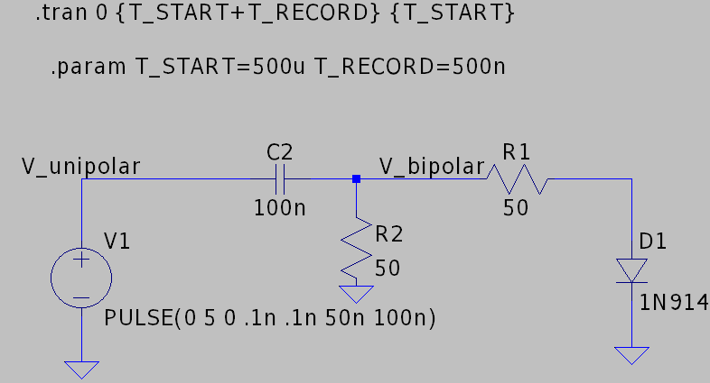
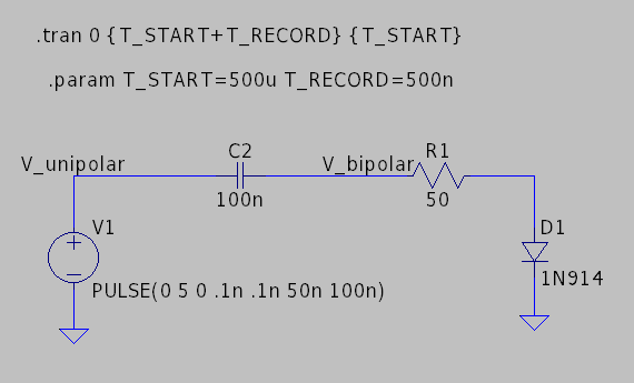
This works OK under linear loads. However, in simulations with switched loads, I'm observing that this is not occurring. See following circuit and simulation result

enter image description here

enter image description here

Voltage signal clearly has a DC value. It is a square wave with levels .5 and -4.5. This is not expected under the assumption that "capacitor blocks DC". However it is seen that current waveform has almost no DC (spikes are +80 mA and -60 mA, average value is 8 uA)

If we add a parallel resistor to allow current to flow through the capacitor when voltage is negative, current waveform is no longer a series of impulses but a "square" wave.

enter image description here

enter image description here

Again, voltage HAS a DC component, while current doesn't (~200 uA average value)

What I conclude from this, is that a series capacitor works as DC block FOR CURRENT. Voltage waveform will be whatever is needed to sustain the 0-DC current waveform. In the case of linear loads this results in voltages with 0-DC, under switched loads (like this case) not necessarily. Is this correct? Or is the effect that I'm observing in this simulations something else?

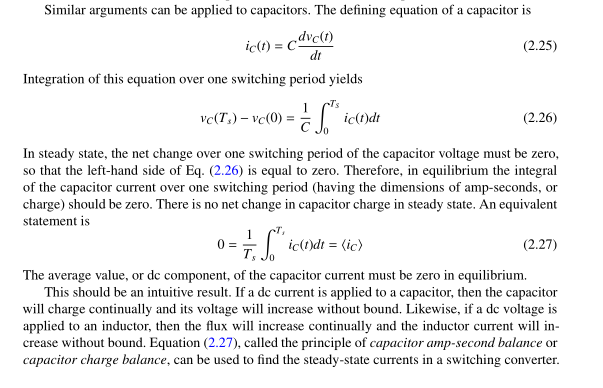
As a theoretical basis, an ampere-second balance for a capacitor in steady state is presented in Fundamentals of Power Electronics, in an analogous manner to the volt-second balance in an inductor

enter image description here

\$\endgroup\$
10
  • 1
    \$\begingroup\$ The diode can only conduct current in one direction so there is no way you can measure a voltage with no DC component. \$\endgroup\$ Commented May 16, 2022 at 23:36
  • \$\begingroup\$ "Voltage signal clearly has a DC value". No, not really. The idea that a signal is separable into portions existing at different frequencies assumes the superposition principle, which only holds for linear systems. Mathematically, you can still perform a frequency decomposition of the signal and claim to find "the DC aka 0 Hz" component, but that component is utterly meaningless in the analysis of a circuit with non-linear elements such as diodes. \$\endgroup\$
    – Ben Voigt
    Commented Jul 3, 2023 at 19:13
  • \$\begingroup\$ @BenVoigt the idea that a signal is separable into a superposition of sinusoidal waves depends on the signal being L1 i.e. absolutely integrable. That depends just on the signal, and not on how it was generated. So it is 100% valid to do fourier analysis of the signals and analyze its components. Being the circuit non-linear, it is not valid to derive a transfer function from those signal transformations, but the frequency analysis is totally valid. \$\endgroup\$
    – MPA95
    Commented Jul 4, 2023 at 14:58
  • \$\begingroup\$ @MPA95: That's why I said "Mathematically, you can still perform a frequency decomposition of the signal" ... but ... "is utterly meaningless in the analysis of a circuit with non-linear elements" \$\endgroup\$
    – Ben Voigt
    Commented Jul 4, 2023 at 15:09
  • \$\begingroup\$ @BenVoigt it is not meaningless at all. If you connect the output of the circuit (any non linear circuit actually) to an ideal opamp with infinite input impedance, then filter the opamp output with an ideal brickwall filter you will recover the DC component (or any part of the spectrum you want), so it is not meaningless at all. Again, what you CAN'T do being the circuit non linear, is perform a linear transfer function analysis. \$\endgroup\$
    – MPA95
    Commented Jul 4, 2023 at 17:04

2 Answers 2

1
\$\begingroup\$

Your circuit has a DC voltage on the right hand side of the capacitor because the diode shunts away part of the voltage during part of the cycle. In essence, the diode is taking what would otherwise be a signal with 0 DC voltage and rectifying it (in a way), this creating a DC component to the signal.

\$\endgroup\$
5
  • \$\begingroup\$ Yes, but note there is a resistor between the diode and the capacitor... so yes the node between the resistor and diode should be shunted to the ~0.7 V of the diode... but that in principle does not shunt the capacitor node... \$\endgroup\$
    – MPA95
    Commented May 16, 2022 at 22:57
  • \$\begingroup\$ Sure it does. If the right hand side of the resistor has a DC component to it's voltage, the left side will usually as well. \$\endgroup\$ Commented May 16, 2022 at 23:06
  • \$\begingroup\$ If you were to add another resistor and diode to the capacitor node, but with the diode reversed, then the DC at the capacitor node would fall to zero or close to it. The two DC components from the two resistors would cancel out, like a voltage divider. But since you don't have a cancelling DC, you see some DC at the capacitor node. \$\endgroup\$ Commented May 16, 2022 at 23:11
  • \$\begingroup\$ I believe that the configuration you are proposing will result in a 0-DC voltage waveform as you are saying, but because the configuration allows for a symmetrical current waveform with symmetrical voltage waveform. I'm not following your reasoning on the DC components \$\endgroup\$
    – MPA95
    Commented May 16, 2022 at 23:17
  • \$\begingroup\$ My understanding of one of your comments is that the resistor should provide isolation for the capacitor from the rectifying effects of the diode. I am arguing that a resistor will only isolate the DC component if there is a correspondingly opposed DC applied to the capacitor node. Without that opposing DC, the resistor will not prevent the DC that appears on one of its terminals from causing a DC component to appear on the other terminal. \$\endgroup\$ Commented May 16, 2022 at 23:25
0
\$\begingroup\$

Think about the basics that depend on time constants and duration and the possible differences between your schematic and your actual circuit that would cause 50 to 100 mA current spikes on each edge of plot 1.

(Note to all LTspice users, please get rid of blue plots and use better labels that match the schematic !)

  • After some time after t=0 the cap will be charged up with a small Vf drop on the diode 0.4 and -ve pulse = -4.6V.

What will cause spikes in the diode current? (seen by series cap current Ic.)

Answer: Junction Capacitance

What should the peak current spike be anyhow with a few pF across the diode symbol?

  • almost 5V /50 = 100 mA. What are you reading in blue 40? to 80 mA? Measurement error and schematic is logically incorrect without a junction capacitance note. However, diode capacitance increase towards the threshold of conduction and decreases with Vr, so it isn't constant but if the ESR of the diode capacitance is small relative to the 50 Ohms, you should always see almost a 100 mA current spike but now spewing noise up to the GHz range.

  • The second plot loads the AC coupler to remove all DC faster because the diode is a high impedance in reverse bias. Now the Cap current sees 25 Ohms for positive current and 50 Ohms for negative current, so it is more like a symmetrical square wave current and the diode capacitance is still there for the negative spikes and on top of the offset square currents, but hard to see due to the LTspice plot resolution and colours but now you see some 4 ns effects of reverse recovery time. (check if that is valid on the datasheets)

Although Falstad's browser JS simulator does not model diode capacitance, it does a better job with plotting results on all parts.

\$\endgroup\$

Your Answer

By clicking “Post Your Answer”, you agree to our terms of service and acknowledge you have read our privacy policy.

Not the answer you're looking for? Browse other questions tagged or ask your own question.