4
\$\begingroup\$

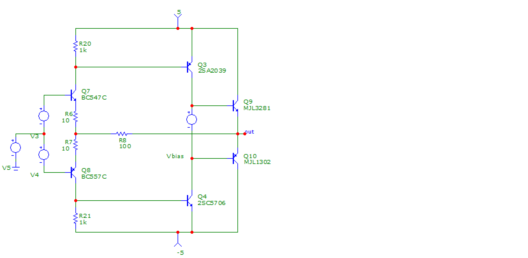
For a personal project, I'd like to make a discrete current feedback opamp. Here's a simplified schematic:

enter image description here

The question is about how to bias Q3/Q4.

For a nice class-AB output, the sum of both Vbe's should be constant. In a common collector output stage (like Q9/Q10), that's easy enough since both Vbes are on top of each other, all that's needed is a bias voltage generator that follows their temperature drift.

But in the common emitter configuration (Q3/Q4), these Vbe's are quite far away from each other. How to keep their sum constant? The usual solution is to put emitter resistors and run them at high bias current, but that means high idle dissipation and low gain.

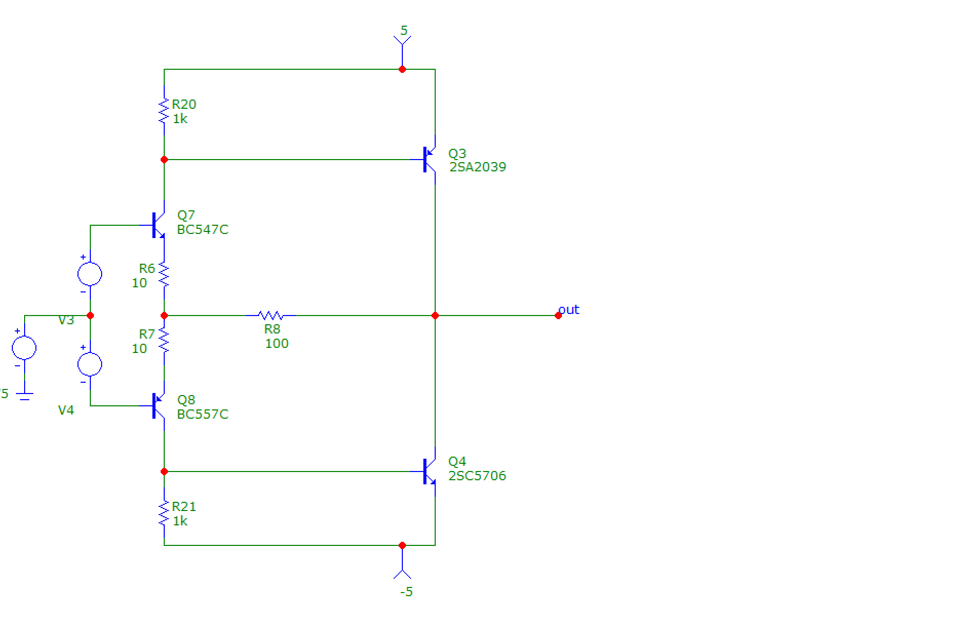
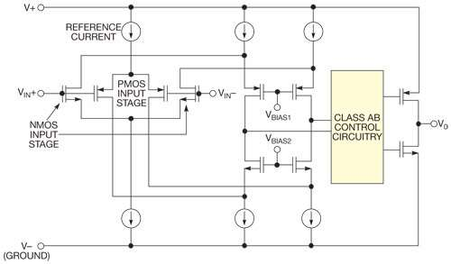
There are plenty of integrated rail to rail output opamps. If I remove Q9/Q10 and squint a little, the schematic looks very much like a rail to rail output current feedback opamp.

enter image description here

So how do they do it? How to bias Q3/Q4 so they run in class-AB without the current running away?

Usually datasheets show a magic box, they're not telling about the secret sauce inside...

enter image description here

\$\endgroup\$
2
  • \$\begingroup\$ Take a look at the OPA2363 datasheet. Their is an actual detailed schematic of the drive block..It is rather simple. BUT only simple when made in IC form where all those diode drop voltages are matched. Building this in discrete form, you are right back in Class AB knives edge hell. I hate class AB for this reason. I would never have faith in it unless i surround it with sensors and feedback stuff \$\endgroup\$
    – tobalt
    Commented Jul 10, 2022 at 13:40
  • \$\begingroup\$ That's a good one! Thanks. I agree this is not possible to do with discrete components. It's possible to hold a class AB push pull output stage stable without any emitter resistors up to a Vce of say 10 volts and bias up to 100-200mA. I simply soldered the temperature sensors, which were MELF diodes, on the metal tab of the power devices. I plan on trying other methods. \$\endgroup\$
    – bobflux
    Commented Jul 10, 2022 at 20:27

2 Answers 2

4
\$\begingroup\$

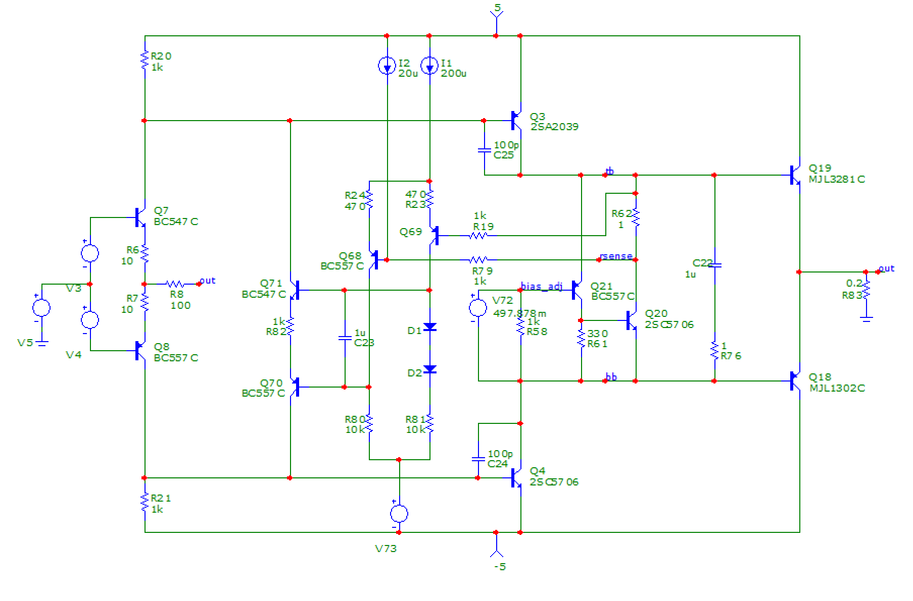
First attempt at self-answer:

enter image description here

Q20-Q21 make a shunt regulator that biases the output transistors Q18-Q19 (thermal compensation not shown). Q68-69 measure the current through this via R62 and tweak Q70-Q71 to adjust the driver transistors Q3-4 so the average current through the aforementioned shunt regulator remains civilized. C23 should correspond to the thermal time constant of said transistors.

This would not work in an opamp which has to process DC signals.

It works perfectly (ie, Q3-4 are biased as I wanted them) but it also doesn't work at all: the output THD is not better than an EF2 output without further complications.

I'm still interested in how the output stage of a RRO opamp is biased, though.

\$\endgroup\$
2
  • \$\begingroup\$ so essentially you replaced R4 in my answer with another opamp supply current and take the output biasing current as input to this opamp. Why wouldn't it work in am integrated part ? \$\endgroup\$
    – tobalt
    Commented Jul 1, 2022 at 20:10
  • 1
    \$\begingroup\$ It would probably work in an IC but it is based on averaging, so it can only process AC signals centered on zero current. An opamp that can't process DC signals would probably not sell... \$\endgroup\$
    – bobflux
    Commented Jul 1, 2022 at 20:36
3
\$\begingroup\$

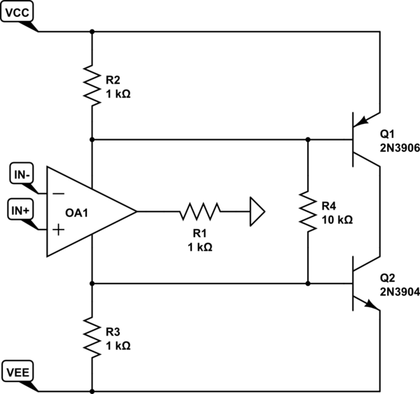
The general idea is below, the IN+/- are the differential outputs of the input differential stage. Global feedback assures that these two inputs are identical in equilibrium and thus the ground current of OA1 is ~0.

In this case, the quiescent current of OA1 and R4 current keep the output transistor on the Class-AB knive's edge.

The resistor values still must be finetuned for the amplifier to neither succumb into class B mode nor run hot with excessive dissipation. I guess rail-to-rail ICs have more circuitry to prevent the runaway.

schematic

simulate this circuit – Schematic created using CircuitLab

\$\endgroup\$
3
  • \$\begingroup\$ Hmmm, yeah I know that one. But that leaves out the tricky matter of biasing the two transistors. Usually there's emitter resistors to make it easier... \$\endgroup\$
    – bobflux
    Commented Jul 1, 2022 at 18:29
  • \$\begingroup\$ @bobflux I see. Well make it clear in your question (can refer to this post as a non-answer ;) ). I would also be interested in how to do it better, because as you realize from my text, the biasing of this structure is hard. \$\endgroup\$
    – tobalt
    Commented Jul 1, 2022 at 18:31
  • \$\begingroup\$ I've found a solution! But it's disappointing. \$\endgroup\$
    – bobflux
    Commented Jul 1, 2022 at 19:15

Your Answer

By clicking “Post Your Answer”, you agree to our terms of service and acknowledge you have read our privacy policy.

Not the answer you're looking for? Browse other questions tagged or ask your own question.