2
\$\begingroup\$

In chapter number 6, page number 428, of the book "ANALYSIS AND DESIGN OF ANALOG INTEGRATED CIRCUITS" by Gray, Hurst, Lewis & Meyer there is a statement:

In MOS technologies, however, the \$g_m r_o\$ product is usually between about 20 and 100, reducing the gain per stage and sometimes causing the offset of the second stage to play an important role in determining the op-amp offset voltage".

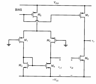
Below I have attached the image of the 2-stage op-amp. enter image description here

What I understand about offset voltage is that it is the differential input voltage for which the output voltage is '0' and in a non-ideal op-amp the offset voltage is present due to mismatches in the input transistors. What I am not understanding that how the offset voltage is related to intrinsic gain? And how can we say that a small intrinsic gain between 20 to 100 reduces the gain per stage?

\$\endgroup\$
4
  • \$\begingroup\$ Sir I have edited the question. Is it ok now? \$\endgroup\$
    – Arnab Deb
    Commented Jul 7, 2022 at 12:36
  • \$\begingroup\$ Maybe post the quote as a picture. \$\endgroup\$
    – Andy aka
    Commented Jul 7, 2022 at 12:41
  • 1
    \$\begingroup\$ @Andyaka I fixed it {facepalm} \$\endgroup\$ Commented Jul 7, 2022 at 12:56
  • \$\begingroup\$ So I gather that when you say "intrinsic gain" you mean \$g_m r_o\$ -- could you clarify that in your text? Even if it's just changing "intrinsic gain" to "intrinsic gain (\$g_m r_o\$)"? \$\endgroup\$
    – TimWescott
    Commented Jul 8, 2022 at 14:31

3 Answers 3

4
\$\begingroup\$

This is basic feedback stuff.

The diagram shows a model of an op-amp that shows just the parts of the problem that concern us here. \$v_i\$ is the "usual" first-stage input offset that you're thinking about. \$H_i\$ is the first-stage gain, \$v_m\$ is the offset voltage of the intermediate stage, and \$H_o\$ is the gain of the rest of the op-amp.

Block diagram of op-amp showing offsets

For the moment, consider \$v_i\$ to be zero. Then, for the output to be zero, \$v_m\$ must be overcome. For that to happen, the input differential voltage must be equal to $$\frac{v_m}{H_i} \tag 1$$.

If by "intrinsic gain" you mean the transistor's intrinsic gain, \$g_m r_o\$, then your \$H_i\$ will, at DC, roughly equal \$H_i \simeq g_m \frac{r_o}{2}\$*, or half of the \$g_m r_o\$ product.

That is why the intrinsic gain matters. Look at (1) and ask what happens as \$H_i \to \infty\$. Now look at (1) and ask what happens as \$H_i \to 1\$. Your question should be answered.

* Analyze the circuit behavior around M1-M4. It should be clear. Note that I may be off by a factor of 2 or 4, but the gain of that stage is -- to a first order -- going to be proportional to \$g_m r_o\$.

\$\endgroup\$
3
  • \$\begingroup\$ Thank you sir for your answer. But I still have a doubt regarding the intrinsic gain.If I quote from the book Analog CMOS IC by B.Razavi "intrinsic gain of a transistor represents the maximum voltage gain that can be achieved using a single device". It has been explicitly written "a single device". \$\endgroup\$
    – Arnab Deb
    Commented Jul 8, 2022 at 6:26
  • \$\begingroup\$ In the diagram that you have shared, you have assumed "Hi" as the intrinsic gain of the 1st stage, but the first stage includes 5 FETs and intrinsic gain is what I have understood is the maximum gain of each of these individual 5 transistors. \$\endgroup\$
    – Arnab Deb
    Commented Jul 8, 2022 at 6:28
  • \$\begingroup\$ The overall gain of the 1st stage is "gm*rout" , where gm is the transconductance of the input transistors and rout is the parallel combination of the drain-source resistances of M2 and M4. So isn't this gain different from the intrinsic gain? \$\endgroup\$
    – Arnab Deb
    Commented Jul 8, 2022 at 6:28
2
\$\begingroup\$

revised

  • Just back from golfing on a course built on a ski slope and I came across an image search/match from a Polish Wikipedia site for the MOSFET which gives a better description of the same schematic.

An unbalanced negative supply is used and Vo+ is actually the offset adjustment to provide the maximum output swing from input Vi-. So the input offset is used to null the output offset to the middle of the asymmetric bipolar supplies.

"let the first stage gain be 50. Then any difference of 50 mV will require an input voltage offset of 1 mV.=

sometimes causing the offset of the second stage to play an important role in determining the op-amp offset voltage"

https://www-wikiwand-com.translate.goog/sh/MOSFET?_x_tr_sl=auto&_x_tr_tl=en&_x_tr_hl=en-US&_x_tr_pto=wapp


Tim's answer looks the best, yet this 7 transistor analog amplifier seems problematic to me with missing assumptions on the common-mode DC input bias which is not provided which determines \$V_{ov}\$.

The differential inputs are common-mode (+,-) to \$-v_{ss}\$ for each input \$v_{o1}, v_{i2}\$.

The gain in any active mode FET is \$g_mr_oR_D\$ where this differential cascode is bias sensitive to determine \$R_D\$ for each stage.

My interpretation is that reducing the over-voltage above Vt threshold to reduce \$g_m\$ reduces the sensitivity to offset voltage.

Yet this Op-Amp is unstable alone and has critical bias needs with only one Vt controlled current source. More popular are the 9 transistor configurations with 3 Vt controlled current sources (where Vgs=Vds).

I think the author was pointing out a weakness of this architecture, which I have yet to see commercially.

I could be wrong as I have not read this book which is the bible of CMOS design started in 1984 now in 5th edition.

Prof Johns has a nice equation sheet to show the dependency of each variable.
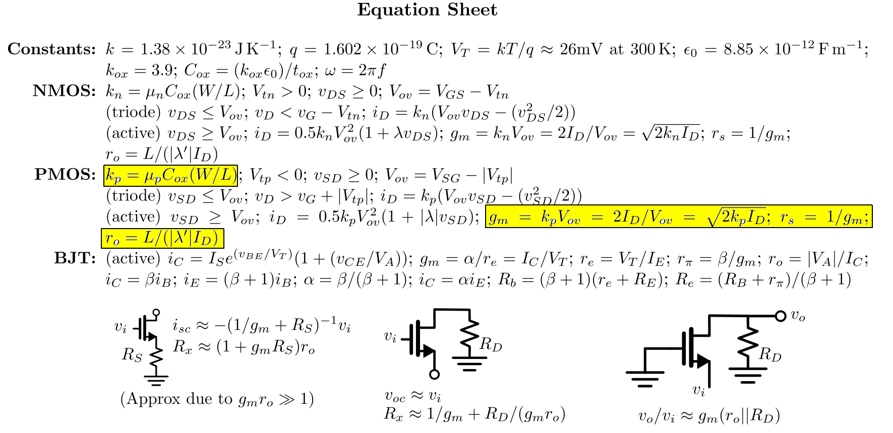
enter image description here https://www.eecg.utoronto.ca/~johns/ece331/problems/equation_sheet.pdf
\$\endgroup\$
3
  • \$\begingroup\$ One hopes that it's a textbook circuit that was drawn for the purposes of illustration. I would assume that there's at least one FET lurking stage left that turns M5 and M7 into a pair of current mirrors (half current mirrors? I'm not sure of the right terminology). \$\endgroup\$
    – TimWescott
    Commented Jul 7, 2022 at 20:02
  • \$\begingroup\$ Yes Sir there is one more FET to the left of M5 forming current mirror for biasing purpose of the 1st stage. \$\endgroup\$
    – Arnab Deb
    Commented Jul 8, 2022 at 6:15
  • \$\begingroup\$ Thank you sir for your answer. The theory given on the website that you have shared is entirely from the book that I have mentioned. \$\endgroup\$
    – Arnab Deb
    Commented Jul 8, 2022 at 6:33
2
\$\begingroup\$

What I am not understanding that how the offset voltage is related to intrinsic gain?

For intrinsic gain I assume you mean this line from your quote:

the \$g_mr_o\$ product is usually between about 20 and 100


If, the 1st-stage gain is 100 and, the 2nd-stage input offset voltage is (say) 10 mV, that offset voltage (when "referred" to the 1st-stage input) is 10 mV/100 = 0.1 mV.

So, if the 1st-stage also has an offset of 1 mV, then the overall offset voltage (including the 2nd-stage referred offset) is 1.1 mV at the input terminals.

In other words the 2nd-stage input offset has only a small effect on the overall input offset of the op-amp when the 1st-stage gain is 100.

On the other hand, if the gain of the 1st-stage is 20, the 2nd-stage offset referred to the input is now 0.5 mV and, this much more significant than when the 1st-stage gain was 100.

You could also refer offsets to the output and you would see that with more gain after an offset, the more significant it becomes as an error term.

\$\endgroup\$

Your Answer

By clicking “Post Your Answer”, you agree to our terms of service and acknowledge you have read our privacy policy.

Not the answer you're looking for? Browse other questions tagged or ask your own question.