7
\$\begingroup\$

AFAIK, Igs of MOSFET/JFET is around 0.

That means that in MOSFET/JFET almost no current flows from gate to drain.

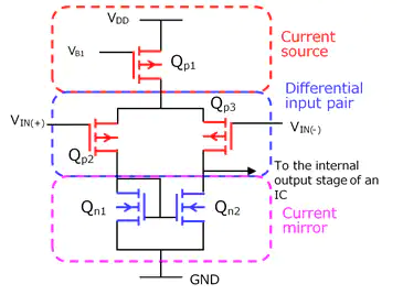
Modern FET input stage:

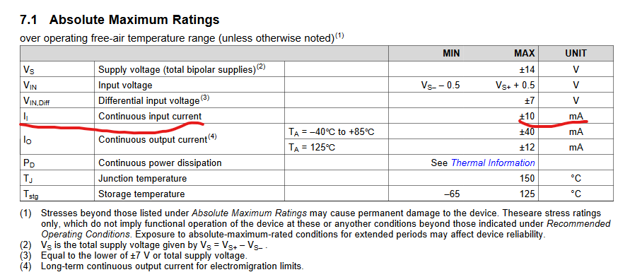
I read some op-amp datasheets, those op-amps have FET inputs, but they still have a max. value for the input current.

For example, the OPA2810:

OPA355:

Theoretically, the FET input stage of op-amps has a current input of about 0, so why does the FET input stage of op-amps still have an input current limit?

\$\endgroup\$

5 Answers 5

15
\$\begingroup\$

Those are absolute maximum ratings.

And it does not mean that current goes through the FET gate, but protection circuitry, such as clamping diodes to VCC and GND.

If you exceed the maximum allowed voltage, the protection diode starts to conduct current to clamp the voltage, and that limit comes from internal wiring including the protection components that should not be exceeded or immediate degradation and/or damage can happen.

The OPA2810 datasheet has a picture (sec. 8.3.2) of how the internal ESD protection diodes are connected.

\$\endgroup\$
5
  • \$\begingroup\$ True that. Too early in the morning for me. I will correct my answer. \$\endgroup\$
    – Designalog
    Commented Feb 25, 2023 at 10:27
  • \$\begingroup\$ There may also be input protection diodes (as in shunting in parallel between inputs). I forget if I've ever seen those on FET or MOS types, but it's something to be very careful about anyway; the inputs may even be rated for full voltage because they put in current-limiting resistors to these diodes, making the amp perfectly useless as a comparator (and questionable as a limiter) while still claiming usefully low input bias current. \$\endgroup\$ Commented Feb 25, 2023 at 14:01
  • \$\begingroup\$ Thanks @Justme's reply. Over absolute max. rate would damage other component, not MOSFET/JFET input pair. \$\endgroup\$
    – curlywei
    Commented Feb 25, 2023 at 15:36
  • \$\begingroup\$ So is the "Latch up" of the MOSFET also caused by the ultra-absolute maximum voltage( or current) value? \$\endgroup\$
    – curlywei
    Commented Feb 25, 2023 at 15:38
  • \$\begingroup\$ Had a very funny awakening about this when the current trough the opamps (INA111) suddenly started to heat my cryostat..... \$\endgroup\$
    – Sascha
    Commented Feb 26, 2023 at 12:55
4
\$\begingroup\$

As others have said that's the absolute maximum current before the device is likely to be damaged.

For the input current under normal operation, that is called input bias current, and this number will likely be indistinguishable from 0 for an op-amp with MOSFET inputs.

enter image description here

350pA - looks indistinguishable from zero to me. and even better at room temperature.

\$\endgroup\$
2
\$\begingroup\$

The max. limit of input current and voltage stated in the datasheet has to do with the reliability and safe operating area for the MOS input stage.

If the user forces more than the state current (meaning, that current has no other way to go than the gate/ESD input circuitry of the input stage), the manufacturer cannot guarantee your amplifier will keep working properly. The diodes will start to conduct, will clamp to a voltage and no useful signal will reach your input gate. You might even break/stress the wiring or ESD circuitry as a consequence.

Also, all MOS transistors need an input current to properly function, however small they are. For a 28nm CMOS process, 5nA of input bias current is not unheard of.

\$\endgroup\$
3
  • \$\begingroup\$ 5nA for a MOSFET input opamp is pretty unheard of, unless you are speaking about rather elevated temperature. At RT, most of them are a few pA max, and that likely is leakage of the protection diodes. \$\endgroup\$
    – tobalt
    Commented Aug 7, 2023 at 19:45
  • \$\begingroup\$ @tobalt I beg to difer. I have seen it in simulation and measured it myself. 28nm is a very unforgiving technology to design chips with. It only gets worse with more advanced nodes. \$\endgroup\$
    – Designalog
    Commented Aug 7, 2023 at 20:11
  • 1
    \$\begingroup\$ Ah yes sorry. @ErnestoG I was thinking of discrete opamp parts made with large analog CMOS processes and thick oxide. \$\endgroup\$
    – tobalt
    Commented Aug 8, 2023 at 15:46
1
\$\begingroup\$

Under your heading

Modern FET input stage:

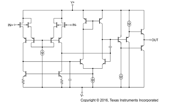
The image in your question is of a MOSFET circuit. As we will see, the behavior of JFETs is somewhat different from those of MOSFETs. For reference, the OPA827 from TI is designed something like this:
enter image description here

AFAIK, Igs of MOSFET/JFET is around 0.

That means that in MOSFET/JFET almost no current flows from gate to drain.

MOSFETs and JFETs have almost 0 gate current under normal operating conditions if the gate voltage is not varying. However, the mechanisms are different.

The gate of a MOSFET is insulated from the channel by an oxide layer. The gate of a JFET under normal operating conditions is insulated from the channel by a depletion layer. It is important to note that this depletion layer is something dynamic, depending upon operating conditions, rather than something static and material, like an oxide layer.

What about under not-so-normal operating conditions?

In an N-channel JFET, if the gate voltage is higher than the source voltage, the depletion layer no longer insulates the gate from the channel. The otherwise high impedance of the gate becomes very low. If current is not limited externally, the gate current may become excessive. However, if there is external current limiting, the JFET may be protected.

In the case of JFETs, a gate voltage which is acceptable when a circuit is powered, may result in a forward biased gate-to-channel junction when the circuit is powered off, but an input signal is still applied. Similar problems may occur in CMOS devices.

In the case of MOSFETs, an excessive gate voltage can "punch through" the thin oxide layer insulating the gate, causing high gate currents and damaging the device.

For either JFET or MOSFET inputs, clamping diodes are sometimes used at the inputs to ensure the gate voltages do not exceed rated maximum. However, the clamping diodes themselves, are subject to failure if they pass too much current. So, current limiting resistors may be helpful to protect the diodes which in turn protect the FETs.
\$\endgroup\$
0
\$\begingroup\$

If your input voltage exceeds the supply voltage, the body diode of the input MOSFET will start conducting when its forward voltage is reached. If you are sensing the voltage of a switched inductor (for example), it will sustain its current momentarily when switched off. If your opamp does not allow for that current, you'll need to clamp the excess voltage/current off using an external Schottky diode in order to keep the body diode from conducting.

\$\endgroup\$

Your Answer

By clicking “Post Your Answer”, you agree to our terms of service and acknowledge you have read our privacy policy.

Not the answer you're looking for? Browse other questions tagged or ask your own question.