1
\$\begingroup\$

I'm using this ECS-240-10-36-CKM-TR part with this IC

The load capacitance mentioned in the crystal datasheet is 10pF and the shunt capacitance is 5pF.

In the design, the load capacitors that I have placed with the IC are 18pF and the design works fine. A stray capacitance of 2pF is considered for the calculation.

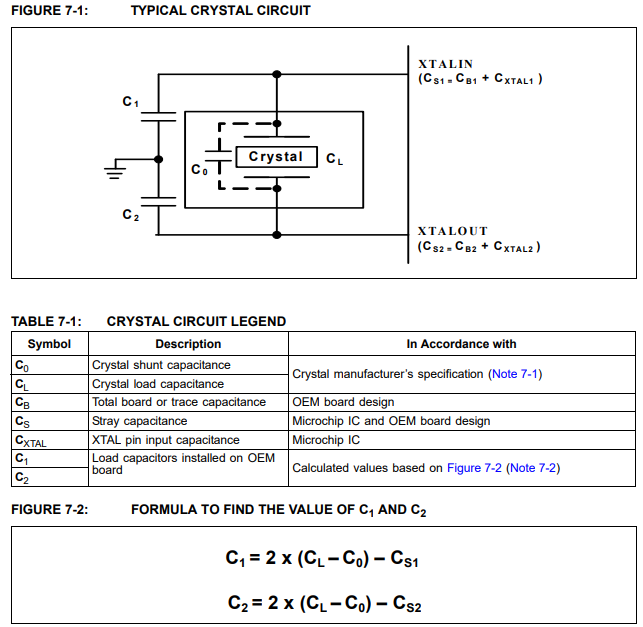
I made this load capacitor calculation considering the below formula from the datasheet.

strong text

What I noticed is that, even without considering the shunt capacitance value of 5pF (as mentioned in the crystal datasheet), I calculated the value of load capacitors which turned out to be 18pF, and started working with this design.

Considering the shunt capacitance (5pF) of the crystal in the formula, the value of the crystal load capacitors comes to around 8pF. But I placed 18pF. There is a significant difference, right?

Now, my question is, the equation from the datasheet mentions including the shunt capacitance in the formula for load capacitor calculation. Whereas, I calculated the value of load capacitors without considering the shunt capacitance. But the design seems to be working.

Would there be any problem in the future?

\$\endgroup\$
15
  • \$\begingroup\$ The shunt capacitance shouldn't be part of the formula in the data sheet. Personally, I think they are wrong. \$\endgroup\$
    – Andy aka
    Commented Apr 24, 2023 at 7:12
  • \$\begingroup\$ @Andyaka Oh, I saw somewhere that usually, the crystal manufacturers include the value of shunt capacitance in the load capacitance value itself. So, any idea whether my value of 18pF is fine? The immediate layer beneath the crystal traces is ground and the prepreg is 3.4mils thick. \$\endgroup\$
    – user220456
    Commented Apr 24, 2023 at 7:14
  • \$\begingroup\$ Not as far as I'm aware. Follow the crystal data sheet and use 10 pF loading. I expect that someone in the data sheet department for the IC thought they knew what they were on about. \$\endgroup\$
    – Andy aka
    Commented Apr 24, 2023 at 7:15
  • \$\begingroup\$ But 18pF is working @Andyaka \$\endgroup\$
    – user220456
    Commented Apr 24, 2023 at 7:16
  • 1
    \$\begingroup\$ @Newbie Both formulas are correct. The difference is, how you calculated all the stray capacitances together into a single Cstray value, i.e. are the strays separate and parallel to C1 and C2, or are the strays already considered as parallel shunt between crystal pins. The definition what are meant by the strays is important, so you know which formula to use. \$\endgroup\$
    – Justme
    Commented Apr 24, 2023 at 9:46

1 Answer 1

2
\$\begingroup\$

The load capacitance mentioned in the crystal datasheet is 10pF and the shunt capacitance is 5pF

The Microchip document appears to factor-in the internal shunt capacitor of the crystal but, the information presented in the question is without full context. If you read below the featured extract you will see this: -

enter image description here

So, despite erroneously appearing to take account of the crystal's shunt capacitor, the Microchip document redeems itself by advising the reader to assume it is zero.

In other words, if the crystal supplier says that the crystal works optimally with 10 pF of loading capacitance then this will trump the information given in the chip supplier data sheet.

So, 10 pF of loading capacitance ensures optimal frequency accuracy of the crystal. It also sets the correct operating power level for the crystal. I trust the crystal supplier's data sheet.

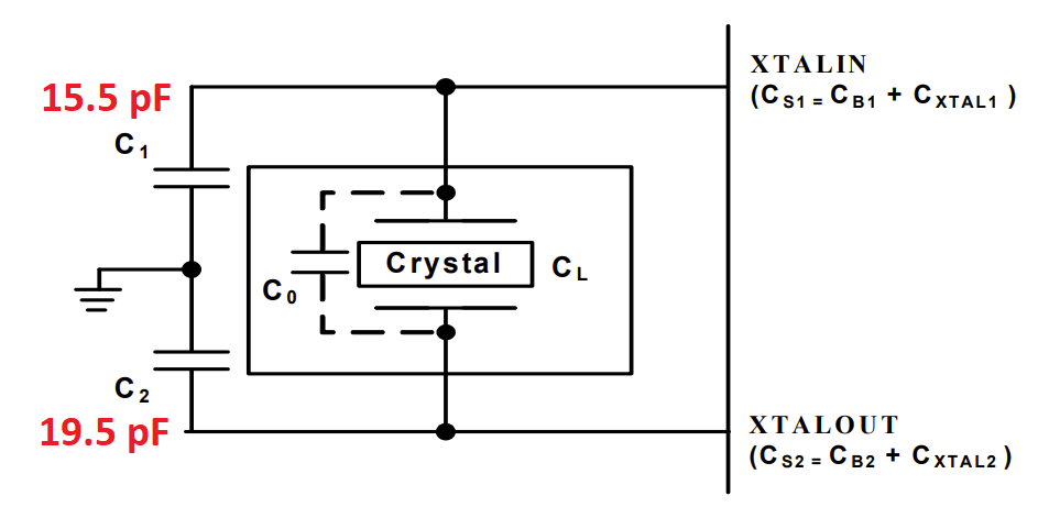
To get 10 pF of loading requires 20 pF capacitors to 0 volts on either side of the crystal. But, you need to take into account stray capacitance of the tracks on the PCB and the input capacitance of the Microchip device. It's likely that the input capacitance of the chip is about 4 pF (check to see if the data sheet mentions this). If the data sheet is weak in this area then you should consider contacting Microchip.

I expect that the parasitic capacitance of the PCB tracks are going to be about 0.5 pF (not 2 pF) but, you can calculate this more thoroughly.

So, based on 4 pF input capacitance and 0.5 pF track capacitance, you would naturally choose values shown below in red: -
enter image description here

But, it won't be too far out if you averaged both out to be 17.5 pF and, of course, 18 pF for each side won't be a show-stopper.


Extra section

Having fully read the Microchip document, the XTALIN capacitance is stated as being 6 pF: -

enter image description here

Absent from that table is any mention of the XTALOUT capacitance and, there's a reasonable explanation for this. That explanation is that the series output resistance of that pin dictates performance. A series output resistance is fundamental to how these types of crystal oscillators work. The value will be a few tens of ohm up to several hundreds of kΩ (for wrist-watch crystals). For this chip it might be around 20 or 30 Ω and, any parasitic capacitance might be a couple of hundred femto farads (negligible).

So, given all I've said in this added section, you might be tempted to lower the input capacitance to 13.5 pF and keep the external output capacitance at 19.5 pF for absolute best crystal frequency accuracy. If clock accuracy isn't a massive factor then stick with 18 pF on each pin to 0 volts. If an accurate clock frequency is important then make the input capacitor 15 pF.

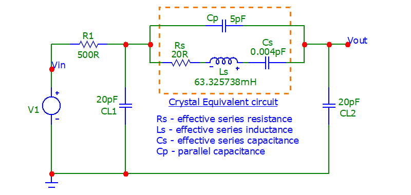
For a little more context on how much a crystal's frequency is affected by loading capacitance, I've added a couple of images from my basic website. The top image is the equivalent circuit of a crystal that has precisely 10.000000 MHz series resonance: -
enter image description here

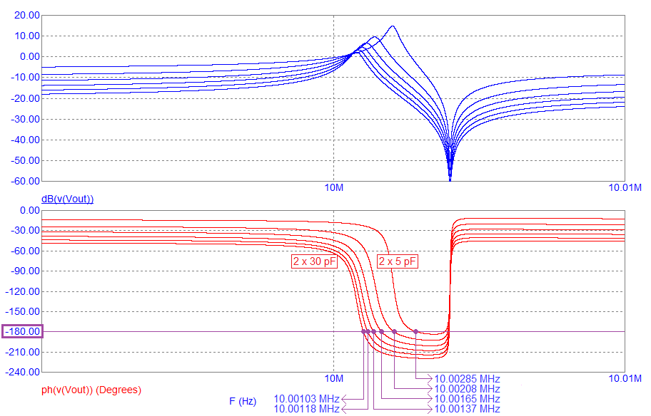
The "loading capacitors" are CL1 and CL2. The XTALOUT ESR is R1. This shows how much the crystal's frequency can vary with different loading capacitors: -
enter image description here

The bottom line is that you might see something like a +/-200 Hz change across a significant range of tuning capacitors. I can't tell you if this might be too much of course.

\$\endgroup\$
4
  • \$\begingroup\$ Why is the IC pin capacitance assumed to be on one pin but not on the other? \$\endgroup\$
    – Justme
    Commented Apr 24, 2023 at 10:58
  • 1
    \$\begingroup\$ @Justme because the driver output (XTALOUT) and its very-necessary effective series resistance (needed for an accurate clock frequency) presents a very low effective capacitance. \$\endgroup\$
    – Andy aka
    Commented Apr 24, 2023 at 11:04
  • \$\begingroup\$ So I guess every datasheet and application note ever made to include the pin capacitance of chip internal IO pin structures for both input and output pins are wrong then. \$\endgroup\$
    – Justme
    Commented Apr 24, 2023 at 11:13
  • 1
    \$\begingroup\$ If a device has dedicated pins for a XTAL then they won't be IO pins. I accept that an MCU that can use IO lines for driving a crystal will have more similar (and greater) input and output capacitance @Justme \$\endgroup\$
    – Andy aka
    Commented Apr 24, 2023 at 11:16

Your Answer

By clicking “Post Your Answer”, you agree to our terms of service and acknowledge you have read our privacy policy.