1
\$\begingroup\$

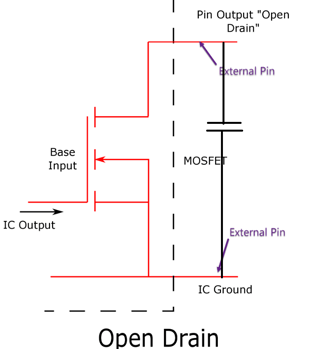
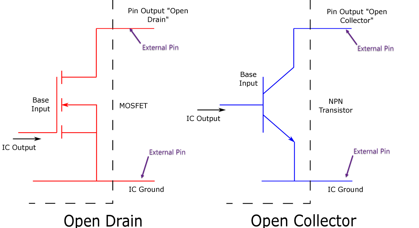
As we know the open drain/collector output stage of a comparator looks something like this:

enter image description here

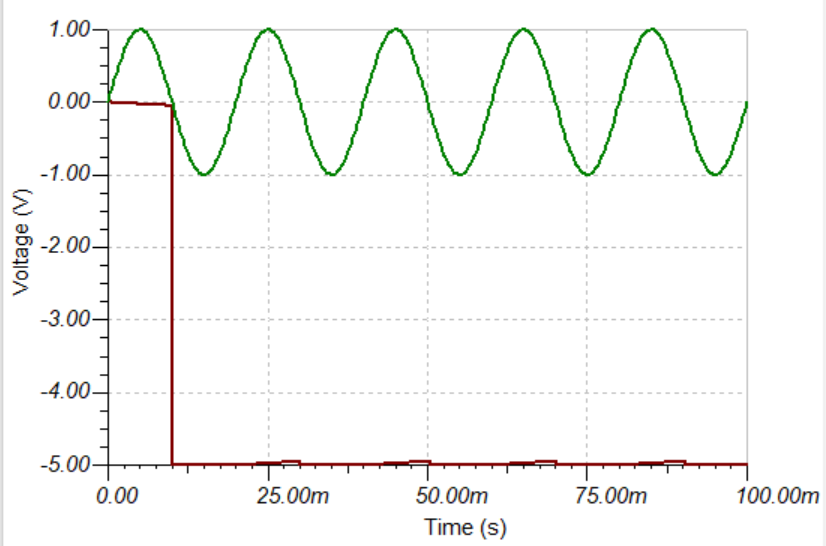
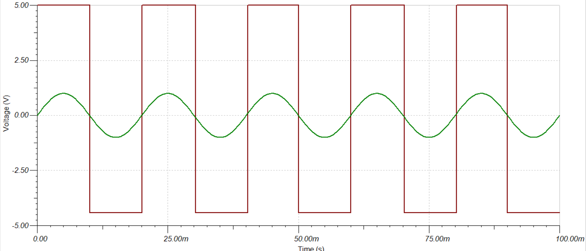
This is essentially a high impendance floating node. If we fail to connect pull up, the output does not go high, however it does go low anytime comparator does (i.e the output MOSFET/BJT gets turned on). This is verified in simulation as well:

without pull-up

Output without pull up

with pull up

Output with pull up

However what I don't get is how could the output stage MOS/BJT possibly get turned on in low state without pull up since the drain/ collector terminal is floating? Where is the path for current flow? Its essentially a MOS/BJT with only gate/base and source/emitter connected.

\$\endgroup\$
6
  • \$\begingroup\$ Which comparator and how did you simulate it? \$\endgroup\$
    – Justme
    Commented Jun 4, 2023 at 19:58
  • 1
    \$\begingroup\$ It's not clear what your concern is. You don't ask about the voltage (e.g. varying degrees of "low"; you might specify more carefully what you mean by "low" however, in terms of absolute voltage, or node resistance, or etc.) so it seems you're satisfied that "low" is "low". Is your confusion basically: "can a switch be said to be 'on' if it has zero volts across it"? \$\endgroup\$ Commented Jun 4, 2023 at 22:33
  • \$\begingroup\$ You should use open drain with resistor. In some cases the resistor is not needed especially if you care about output current (not voltage). In that case the resistor is no needed but it is a good manner to always use some resistor. \$\endgroup\$ Commented Jun 4, 2023 at 22:50
  • \$\begingroup\$ @TimWilliams, by low I meant basically 'ON'. My confusion is, how can the transistor be on with one node floating? \$\endgroup\$ Commented Jun 10, 2023 at 18:11
  • 1
    \$\begingroup\$ When the transistor is "on" (base/gate high) then you can think of the collector-to-emitter (drain-to-source) as a very low ohm resistor. So your question is essentially, "if there's a low ohm resistor to ground on a floating net, where is the path for current flow?" \$\endgroup\$
    – td127
    Commented Jun 11, 2023 at 22:04

8 Answers 8

5
+25
\$\begingroup\$

Let us take the example of the MOSFET with open drain.

There are 2 cases:

  1. When VGS << VTH, the drain terminal is indeed a high impedance floating node
  2. When VGS >> VTH,, the drain terminal is not a floating node. In this case, there is a low impedance between the drain and source.

enter image description here

Assume initially VGS << VTH and the drain is sitting at 0V according to your simulation without pullup. Basically, you can visualize this situation as a capacitance across drain-bulk junction as shown which is holding a charge of 5V (drain voltage = 0V and bulk/source voltage = -5V). Subsequently, when VGS >> VTH the drain-source becomes a low impedance and hence discharges the cap fully. Thus, the drain voltage becomes equal to the source voltage i.e. -5V.

Essentially, the pullup resistor is only needed to pull the drain high. To pull the drain low, we just need VGS >> VTH to be satisfied. If there is no pullup in this case, the drain capacitance will get discharged and eventually drain voltage = source voltage

When Vgs>Vth, channel inversion happens and hence there is a path available for the current. If there is a path available for current, it is low impedance. Drain to source is hence low impedance but drain to supply is high impedance because it has no path to supply.

\$\endgroup\$
2
  • \$\begingroup\$ Basically I am trying to understand the physics behind how impedance can go low with Vgs>Vth with drain floating. \$\endgroup\$ Commented Jun 17, 2023 at 16:29
  • \$\begingroup\$ When Vgs>Vth, channel inversion happens and hence there is a path available for the current. If there is a path available for current, it is low impedance. Drain to source is hence low impedance but drain to supply is high impedance because it has no path to supply. \$\endgroup\$
    – sai
    Commented Jun 17, 2023 at 16:48
1
\$\begingroup\$

I once thought about that one and eventually explained it to myself in the following way.

There is a collector resistor, the open circuit can be viewed as a very very high value collector resistor.

When the transistor's base signal goes active, the transistor tries to switch on and cause a collector current to flow, Ic = beta*Ib which is the maximum collector current that can be achieved. The collector current causes a voltage drop across the collector resistor and the collector voltage falls. If the collector resistor is high enough in value the transistor will saturate and the collector current will be limited to approximately Vcc/Rc. This is what we call a forced beta situation where beta (Ic/Ib) has a value less than the data sheet specified value.

So in your comparator situation there is effectively a very very high collector resistor and a very low forced beta (very low collector current), the transistor is doing its best to achieve the data sheet specified beta and as a result the transistor is saturating. The collector voltage can't rise because the transistor is doing its best to achieve that data sheet specified beta and a rising collector voltage would be reducing beta even further away from what the transistor is trying to achieve.

\$\endgroup\$
1
\$\begingroup\$

It goes low, because when the output transistor is activated, you short the output node to the negative supply.

It is no longer floating in this case, but actively driven low. It only starts to float again, once the output transistor is turned off.

\$\endgroup\$
1
\$\begingroup\$

When the open-collector transistor is turned off, the output doesn't "go low", it just doesn't go High.

When the transistor is on, it actively pulls the output low, but when it turns off, it just lets go of the output - the output will stay low, unless there is something else, like a pull-up resistor, to move it away from the low state.

With the transistor off, if you measure the output voltage to Ground with a DVM, the resistance of the meter will pull the output low, and the meter will read close to Zero. If instead you measure the voltage between the output pin and Vcc, the meter resistance will pull the output up towards Vcc, and the meter will again read near Zero.

\$\endgroup\$
1
\$\begingroup\$

Short answer: for the BJT output, it’s actually the base-emitter current that turns on the transistor, not collector current. Likewise, for the FET it’s the gate-source voltage, not gate-drain voltage.

A way to think of it is take note of the impedance of the open-collector / open-drain signal without benefit of a pull-up:

  • BJT with Vbe in forward bias: collector is low impedance
  • BJT with Vbe not forward biased: collector is high impedance.

Same thing with the FET with its gate-drain voltage in its on and off state.

Now, the thing about the impedance behavior is that it doesn’t care about the actual voltage of the driven line (within limits, see below.)

In both cases, BJT and FET, when the driver transistor is off, the line floats. What it floats to depends largely on what’s attached to it.

If it’s just capacitance, without any other influence it will remain near your negative rail, left over from when the driver was ‘on’, just like your simulation.

If anything, the output driver’s slight off-state leakage will keep the line near the (-) rail. That is, the output driver’s ‘off’ impedance is high, but it’s not infinite.

About that ‘within limits’ above. The off-state transistor or FET will still clamp the output to the (-) rail if for some reason the line tries to go below the rail. This is because both the BJT collector and the FET drain have diode paths:

  • BJT: collector-base is a PN junction that will forward bias when Vcb is -0.5V. Current path will be from base to collector.

  • FET: there is a parasitic diode between source and drain, which will conduct if Vds is -0.5V. Current path will be from drain to source.

In other words, you will see no more than one diode drop below ground, or whatever the (-) supply pin is.

\$\endgroup\$
2
  • \$\begingroup\$ Bjt with Vce in forward bias is low impedance: I don't get this, how can it be forward biased if the collector is not connected. It's essentially npn junction with only p and n supply connected. \$\endgroup\$ Commented Jun 17, 2023 at 7:44
  • \$\begingroup\$ Meant to say Vbe. Corrected. \$\endgroup\$ Commented Jun 17, 2023 at 19:37
1
\$\begingroup\$

My confusion is, how can the transistor be on with one node floating?

The question is incorrectly asked because the transistor is off when the node is "floating" and on when the node is grounded.

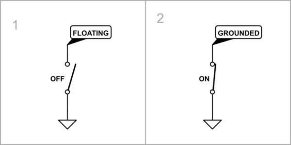
An open-collector (open-drain) transistor stage without a connected "pull-up" resistor can be represented by a simple SPST switch connected through one terminal to ground; its other terminal acts as an output.

schematic

simulate this circuit – Schematic created using CircuitLab

This "configuration" has two possible states:

  1. The switch is off, the output is "floating" (with an unspecified voltage).

  2. The switch is on, the output is grounded (with zero voltage).

So the question "how can the switch be on when the output is floating" makes no sense.

\$\endgroup\$
0
\$\begingroup\$

However what I don't get is how could the output stage MOS/BJT possibly get turned on in low state without pull up since the drain/ collector terminal is floating?

It doesn't get turned on.

Where is the path for current flow?

There is no current flow.

Its essentially a MOS/BJT with only gate/base and source/emitter connected.

And the parasitic capacitance between source/drain or collector/emitter. It is this parasitic capacitance that maintains the low voltage unless it is charged up in some manner. That's what the pullup resistor will do. The time constant with which this happens depends on the time constant for the RC from pullup and parasitic capacitance. Discrete BJTs/FETs usually mention the respective capacitances in their data sheet.

\$\endgroup\$
-1
\$\begingroup\$

If you want to observe the state, you need to connect your circuit and/or a multimeter to it, so there will be some resistance and some capacitance, so some current will flow.

And even if you simulate it with infinite resistance and zero capacitance on the output, the transistor still makes a direct connection to ground. For an active open-collector/-drain output, low is the only possible state.

\$\endgroup\$
2
  • 1
    \$\begingroup\$ "Only possible state" seems misleading. The simulation for example seems to suggest "undefined" is a better description of the non-low state. In IEEE 1164 terms: 'Z'. \$\endgroup\$ Commented Jun 4, 2023 at 22:42
  • 1
    \$\begingroup\$ The staes cannot be defined with voltage or current because nieither are supplied. Instead the states can be defined in terms of resistance: RDSon and RDSoff. RDSon can be estimated from the datasheets. A rough lower bound for RDSoff can be calculated using IDSS andthe test voltge. \$\endgroup\$
    – user319836
    Commented Jun 5, 2023 at 5:26

Your Answer

By clicking “Post Your Answer”, you agree to our terms of service and acknowledge you have read our privacy policy.

Not the answer you're looking for? Browse other questions tagged or ask your own question.