Prerequisites
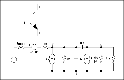
I try to design a radio frequency low noise amplifier with a SiGe transistor (BFP740 infineon.) The amplifier is designed as a common emmiter with inductive degeneration.
Observation
After I optimized for gain and NF I saw that first of all I had to choose a really small value for \$L_{ind., degen.}\$ to get reasonable amount of gain. As far as I understand it, it is possible to enhance the real impedance of the transistor amplifier but I cannot prove this statement.
I could simply match the input to 50 ohm but as soon as I touch the output matching my input matching changes also.
Method
- MWO AWR plotted Gain(2,1) and NF(2,1) while tweaking L
- Matched input to 50 ohm while plotting Zin(1). Then matched output to 50 ohm while plotting Zin(2). After I saw my input changes also I added some elements and matched both to 50 Ohm
Questions
- What is the influence of L? I would be grateful about informations, explanations and formulas.
- What are reasons for the described phenomena? Is it because the capacitance between base and collector connects input to output (S12 is -23 dB).


