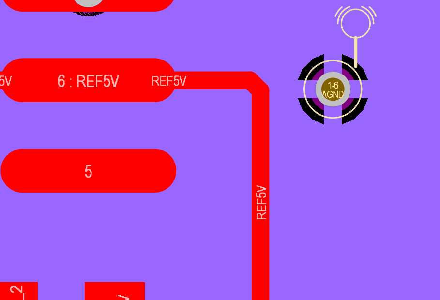
I am connecting a via to a polygon in one of the middle layers. My goal is to use it as a test point. Altium gives me a net Antennae violation. Although there are ways to silent the tool from giving this error, Is this something I should be worried about in terms of PCB performance?
-
\$\begingroup\$ Can you show what is the violation? What is the rule you have setup in rule manager? \$\endgroup\$– mouelleCommented Nov 9, 2023 at 14:19
-
1\$\begingroup\$ Violation is : Net Antennae : Via from top layer to bottom layer. Related rule is: Design rules -> Manufacturing -> Net Antennae -> Net Antennae Tolerance: 0 mil \$\endgroup\$– MoCuishleCommented Nov 9, 2023 at 14:24
-
\$\begingroup\$ You can find the details about net antennae error here: altium.com/documentation/altium-designer/… \$\endgroup\$– liaifat85Commented Nov 9, 2023 at 15:13
-
\$\begingroup\$ I understand why Altium marks this as an error and I can manipulate the rules or manually silent this error. I was wondering if PCB experts could tell me if this is actually going to cause performance issues, or behave like an antennae even though it is only connected to a ground polygon? \$\endgroup\$– MoCuishleCommented Nov 9, 2023 at 15:26
2 Answers
I don't think your via will actually create an antenna.
The net Antenna rule in Altium is to make sure there are no stubs on critical nets. I usually use this rule constraints on high speed interface between a driver and a receiver.
In your case, AGND should not carry high speed signals. The error showed up because you have a thermal relief to your via and this via is not routed to anything (no load). On top of that, your net antenna tolerance is set up to only 0 mils. Hence, this creates a stub and a violation.
On a side note, if you want to reduce stub length on critical nets, you should try to put your test points in-line near the driver or receiver and use backdrilling.
Altium will flag a via going to nowhere as a net antennae. You have two options:
- Right click the error and tell Altium to "waive violations", and ignore it. Altium is warning you that there might be a problem, but the PCB fabricator won't care that you have an untented via to nowhere.
- Replace the via with a pad. The pad will perform the same function as a test point, but without the error.
-
\$\begingroup\$ I mean, you can also just disable the rule, whether by deleting it, disabling it, restricting it to relevant nets/classes, or disabling the rule in Design Rule Check. \$\endgroup\$ Commented Nov 10, 2023 at 16:35

