7
\$\begingroup\$

How does a dual gate MOSFET reduce Miller effect? I am trying to gain a global understaning of the physics behind them, not necessarily exact formula's that come with it other than maybe some for practical use. The Wikipedia article refers to a tetrode article based on tubes, where I get slightly lost.

I guess the questions in order are:

  1. What is a tetrode (in discrete transistor/MOSFET speak);
  2. How is a dual gate MOSFET similar to a tetrode, what are the 'mechanics' behind it in global terms? (Trying to get a feeling for the physics behind it).
  3. How does it reduce Miller effect and is a dual gate MOSFET different from a discrete tetrode in this.
  4. Is a dual gate MOSFET any good for other properties?
\$\endgroup\$
4
  • 1
    \$\begingroup\$ Do you firstly know what miller effect is? Do you know what a cascode amplifier is (this reduces miller effect but uses two discrete BJTs)? Going from two discrete BJT devices to a dual gate mosfet is the best approach to describe because I'm not familiar with tetrode transistors and from what I can gather they were quickly superceded and may not be worth considering. The Tetrode valve however may be worth thinking about because it reduces miller effects pretty much in-line with a DG Mosfet. \$\endgroup\$
    – Andy aka
    Commented May 14, 2013 at 18:47
  • \$\begingroup\$ @Andyaka Great comment, but as a clarification, the Cascode can be built using any type of tube or transistor, even a MOSFET at the Emitter of a BJT, for example: electronics.stackexchange.com/questions/15677/… \$\endgroup\$
    – zebonaut
    Commented May 14, 2013 at 18:57
  • \$\begingroup\$ Yes I'm familiar with Miller effect. Not familiar with cascode. The Wikipedia article disempowered the tetrode valve similarity (especially for impact) \$\endgroup\$
    – jippie
    Commented May 14, 2013 at 19:02
  • \$\begingroup\$ @zebonaut - yes I knew that - i offered up the BJT example because I thought there was more liklihood of the OP being aware of this configuration rather than the JFET or MOSFET version \$\endgroup\$
    – Andy aka
    Commented May 14, 2013 at 20:19

3 Answers 3

9
\$\begingroup\$

I'm going to ignore the reference to tetrode, I have never understood why an exact analogy reveals a fundamental truth.

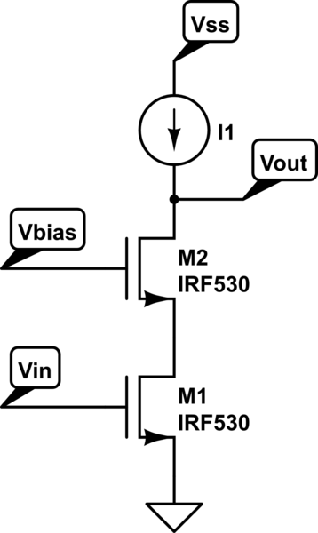
The miller effect arises in situations from a connecting capacitance across two nodes that that have an inverting voltage gain/relationship between them. it doesn't have to be in transistors either, but in MOSFET's you have \$C_{GD}\$. How this is traditionally solved is to cascode the amplifier by isolating the offending capacitance so it doesn't appear across the gain stage. The dual gate Mosfet is basically a cascode stage with the cascode transistor built in (this has a secondary effect, see below), you just have to bias the the transistors so that they are in the active regime. M1 = amplifier, M2 = cascode
schematic

simulate this circuit – Schematic created using CircuitLab

The amplifer transistor converts the input voltage in the output current and the cascode transistor simply transfers this current to the output load. the output is on the drain of the cascode and the input is on the gate of the amplifier transistor. There is no capacitance across the two nodes, the miller effect is greatly reduced.

Cascoding greatly helps in gain too.

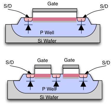
An interesting effect from manufacturing comes into play. The upper device is a longer gate device and the lower is a dual gate device. The S/D implant to channel capacitance tends to be lower than the S/D to isolation edge capacitance (the S/D's on the outer edge) so the S/D in between the gates will tend to have a lower capacitance that if you were to have designed the circuit using two separate transistors in a cascode configuration (and obviously they take up less area). This means that the \$C_{SB}\$ capacitance is less as well making for a higher speed circuit, here SB = Source to Bulk (AKA well).
enter image description here

\$\endgroup\$
3
  • \$\begingroup\$ 'STI edge capacitance' Not sure where to look. Same for Csb \$\endgroup\$
    – jippie
    Commented May 14, 2013 at 20:41
  • \$\begingroup\$ edited to explain terms. STI - Shallow Trench Isolation \$\endgroup\$ Commented May 14, 2013 at 20:57
  • \$\begingroup\$ This speaks for that the capacitance in the drain1/source2 connection point is smaller for a dual-gate compared to two single-gate transistors. Will that give an improvement in bandwidth, though? (compared to two single-gate transistors) Will the bandwidth not be dominated by the (larger) capacitance at the output of the cascode for both the case of a dual-gate transistor and two single-gate transistors? \$\endgroup\$
    – nijoakim
    Commented Jun 3, 2022 at 8:08
1
\$\begingroup\$

A dual-gate MOSFET can be used as a cascode amplifier — see Figure 1 in the Wikipedia article. By holding the "upper" gate at a fixed voltage, the effective drain voltage that the lower gate sees is also fixed, eliminating the effects of capacitive coupling to the lower gate.

\$\endgroup\$
1
\$\begingroup\$

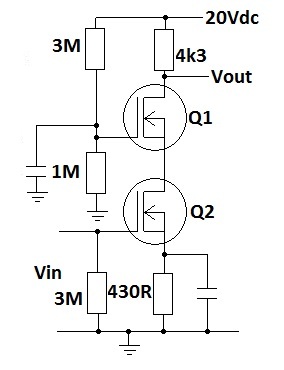
MOSFET cascode: -

enter image description here

Because Q1 has very little AC signal on its source (due to the gate being decoupled), miller effect on Q2 (drain-to-gate) is greatly reduced. Q1 provides the voltage amplification due to it being injected (via its source) with AC current from Q1's drain. Q1 doesn't suffer from miller effect because its gate is decoupled.

Two MOSFETs in a row built on the same substrate is fairly trivial and this forms the dual gate MOSFET which relates to the cascode amp above, and the tetrode valve (which has control and screen gates doing the same thing).

\$\endgroup\$
4
  • \$\begingroup\$ Ported your schematic to circuitlab for better readability, but are these supposed to be P channel MOSFETs? \$\endgroup\$
    – jippie
    Commented May 14, 2013 at 20:27
  • \$\begingroup\$ @jippie I know you meant well but i don't like that circuit - I don't understand the symbol for the N channel FET - it's not what I'm used to seeing so if you wouldn't mind could you please return the original circuit and I'll modify it tomorrow - BTW I can't use the circuit editor on internet explorer, it just will not work on my home PC. If you can't return it back let me know and I'll re-insert it then tomorrow I'll upgrade it to make the n channel device clearer \$\endgroup\$
    – Andy aka
    Commented May 14, 2013 at 20:32
  • \$\begingroup\$ No problem, I commented it back to the original form. I'll see what I did when you edit the question. <!-- and --> \$\endgroup\$
    – jippie
    Commented May 14, 2013 at 20:36
  • \$\begingroup\$ @jippie cheers - might have to ask a question about mosfet symbols on the strength of this \$\endgroup\$
    – Andy aka
    Commented May 14, 2013 at 20:46

Your Answer

By clicking “Post Your Answer”, you agree to our terms of service and acknowledge you have read our privacy policy.

Not the answer you're looking for? Browse other questions tagged or ask your own question.