How is the Gate capacitance and the Miller capacitance modeled for a MOSFET. What is the behavior for both when a Gate Voltage is applied?
-
\$\begingroup\$ What has your research told you so far and don't say "my research has led me to believe that asking the question on EE yields the quickest result". \$\endgroup\$– Andy akaCommented Sep 28, 2013 at 21:46
-
\$\begingroup\$ I did figure out the Gate capacitance part, and how it changes with Current from a MOSFET Driver. But i couldnt figure out the effect on the miller capacitance. I did not ask for the working, just how they are modelled? which i did not come across. \$\endgroup\$– SherbyCommented Sep 28, 2013 at 21:52
-
1\$\begingroup\$ I just caught your comment before you edited it "Thanks for being rude" was the original opening statement in your comment. Made me smile. I think you need to explain what you do know about miller capacitance so that people can answer your question succinctly without any rudeness LOL. \$\endgroup\$– Andy akaCommented Sep 28, 2013 at 22:54
-
\$\begingroup\$ hehe. i didnt wanted to be the same, so i removed it. I dont know much about Miller capacitance, just read on the miller effect and had seen that it causes an apparent increase in the input capacitance, but didnt understand on how its modelled, and if its an effect or is there actually a capacitor there. \$\endgroup\$– SherbyCommented Sep 28, 2013 at 23:11
2 Answers
There is always capacitance between drain and gate which can be a real problem. A common MOSFET is the FQP30N06L (60V LOGIC N-Channel MOSFET). it has the following capacitance figures: -
- Input Capacitance 1040 pF (gate to source)
- Output Capacitance 350 pF (drain to source)
- Reverse Transfer Capacitance 65 pF (drain to gate)
The Miller capacitance is the reverse transfer capacitance listed above and the input capacitance is the gate-source capacitance. Output capacitance is from drain to source.
For a MOSFET, the input capacitance is usually the largest of the three because to get decent throughput (change in drain current for a change in gate-source voltage), the gate insulation has to be very thin and this increases gate-source capacitance.
The Miller capacitance (reverse transfer capacitance) is usually the smallest but it can have a serious effect on performance.
Consider the MOSFET above switching a 10A load from a supply voltage of 50V. If you drive the gate to turn the device on the drain could be expected to fall from 50V to 0V within a few hundred nano seconds. Unfortunately the rapidly falling drain voltage (as the device turns on) removes gate charge via the miller capacitance and this can begin to turn off the device - it's called negative feedback and can result in less than ideal switching times (on and off).
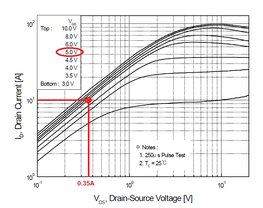
The trick is to ensure that the gate is over-driven slightly to accommodate this. Look at the following picture taken from the FQP30N06L data sheet: -

It shows what you can expect when the gate voltage is 5V and the drain current is 10A - you will get a volt drop across the device of about 0.35V (power dissipation of 3.5W). However, with the drain voltage dropping rapidly from 50V the charge removal from the gate can be such that a third of the gate voltage is temporarily "lost" in the switching process. This is mitigated by making sure the gate drive voltage is from a low source impedance but, if a third is lost, for a short time period it's like having the gate voltage at 3.5V and this dissipates more power in the switching process.
The same is true when turning off the MOSFET; the sudden rise in drain voltage injects charge into the gate and this has the effect of turning the MOSFET on slightly.
If you want better switching then look at the data sheet and over-drive the gate voltage to turn it on and if possible apply negative drive voltage to turn it off. In all cases use low impedance drivers. The data sheet for the FQP30N06L indicates that rise and fall time specs use a 25 ohm drive impedance.
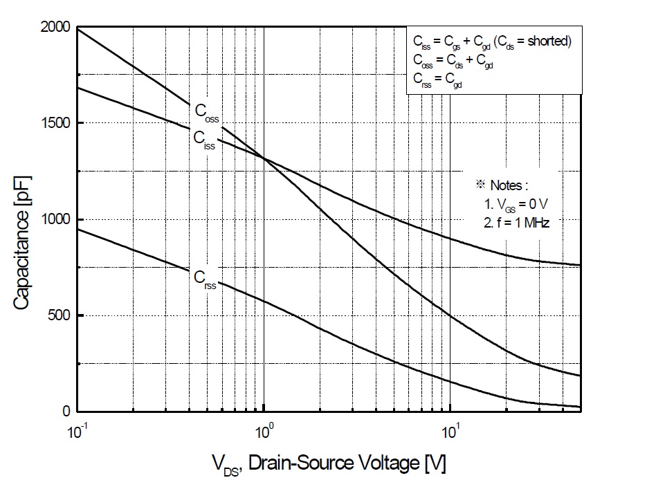
It's also worth mentioning about how the various capacitances are affected by voltage. Look at this diagram: -

For very small drain voltages the miller capacitance (Crss) is nearly 1nF - compare this when the device is turned off (say 50V on drain) - the capacitance has dropped to probably less than 50pF. See also how voltage affects the other two capacitances.
-
\$\begingroup\$ I suspect you have a particular device or size of device in mind for the 100 pF that you claim. \$\endgroup\$ Commented Sep 29, 2013 at 0:31
-
\$\begingroup\$ @rawbrawb No particular device - I should have probably been a little clearer and maybe said in the low 100s of pico farad range. \$\endgroup\$– Andy akaCommented Sep 29, 2013 at 10:20
-
\$\begingroup\$ You can get millering on any device, even just an amplifier. The input stage on an amplifier inside an IC might be only a few fF's of gate capacitance with miller capacitance being on the order of 100 of aF's. Your number may only apply to a specific very large power MOSFET (Hexfet ?) or similar. \$\endgroup\$ Commented Sep 29, 2013 at 14:19
-
\$\begingroup\$ @rawbrawb - I've still targetted MOSFETs but I've revamped the answer. \$\endgroup\$– Andy akaCommented Sep 30, 2013 at 9:31
-
\$\begingroup\$ Good article. Thanks for explaining the effect of Miller capacitance and why we need to over drive the gate of the MOSFET \$\endgroup\$– user50877Commented Aug 7, 2014 at 7:36
I am afraid that the term "Miller" capacitance has not yet been properly explained. It was said that the Miller capacitance would be identical to the drain-to-gate capacitance. I think, this neeeds clarification.
The problem is that the Miller effect (caused by negative feedback) increases the input conductance at the gate (in case of common source configurations). This applies to any conducting element between drain and gate (inside and/or outside the device).
Roughly we can say that the Miller effect apparently increases the input capacitance at the gate by a factor equal to the gain A of the stage, hence: Cin~A*Cdg.
That means - as far as modeling is concerned: The Miller effect is not modeled at all and Cdg is modeled as it is (between D and G). A possible increase due to the Miller effect depends on the particular application.
