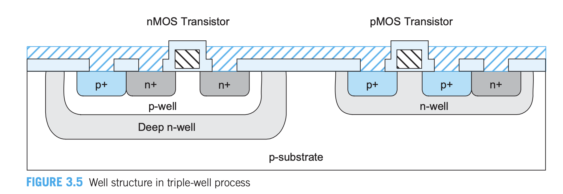
My textbook (Weste and Harris's CMOS VLSI Design) is trying to explain to me the nature of fabricating wells in the twin-well and triple-well processes. My question here is about how we can use so few masks to define these wells.
Weste and Harris claim that
Wells are defined by separate masks. In the case of a twin-well process, only one mask need be defined because the other well by definition is its complement. Triple-well processes have to define at least two masks, one for the deep well and the other for either n-well or p-well.
Question:
In a twin-well process we are defining both p-wells and n-wells (inside, usually, a p-substrate). Don't we therefore need two masks to define these different wells? A similar comment would seem to imply that a triple-well process needs 3 masks?
I suppose my misunderstanding is what they mean by "masks". I am aware that a general process for defining well regions might look like (0) depending on if physical mask or pohotoresist mask can be used, grow thick oxide (1) spin positive photoresist, (2) illuminate regions which are to become wells, (3) develop, (4) if physical oxide mask is used in step 0, etch away exposed oxide regions, (5) implant and anneal. Is the idea of using a single mask that we could subsequently use this same photomask but with negative photoresist, such that when we developed and then implanted (the other dopant type) we would produce the other well type in the region which was previously covered? That is, does "mask" here refer to "photomask", the chromium-plated glass, in that the aforementioned process could use just one of these in order to achieve the desired result? The reason I am skeptical about my guess here is that this aforementioned procedure would guarantee the entire surface of the wafer would be covered by one well or the other, with no space in between them. This is in contrast with the following figure from the text, wherein there is clearly space between the wells:

