0
\$\begingroup\$

Based on Half-Bridge DC-to-DC Converter With Primary-Side Control User's Guide, TI uses the following schematic for driving the synchronous rectifiers on the secondary: enter image description here
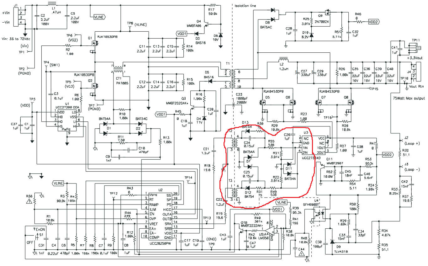
They use a gate drive transformer to pass the signal coming from the primary (from the controller U2) to the secondary, to the gate driver U3. However I don't understand what is going on in between. The pulses coming out of the controller are 12V and the transformer has a turns ratio of 1:1. D7 and D11 are double diodes with common anode. U3 is powered by an 8V supply (VDD2), but what is their purpose in this circuit?

Speaking of VDD2 which is generated in the upper right corner of the image - Will at the start-up of the converter be voltage between pin 6 and 10 of T1, even though the rectifiers are not switching? I believe so, that way they are able to turn on the secondary side too.

Thank you.

\$\endgroup\$
3
  • 1
    \$\begingroup\$ Have you considered simulating the transformers and diode circuits to see how they work? \$\endgroup\$
    – Andy aka
    Commented Jan 4 at 18:46
  • \$\begingroup\$ Yes, but what is confusing me is that the output of the voltage divider R55 & R21 and R49 & R22 is 10V. VCC for U3 is 8V. Pins 1IN and 2IN are the analog input voltage for U3 and according to the datasheet cannot be higher than VCC, but in this case they are (10V>8V)...that is if I interpret the schematic correctly. \$\endgroup\$
    – PosFLo
    Commented Jan 5 at 9:28
  • \$\begingroup\$ What would be the current into the pins and, would that current be more that that allowed in the data sheet (with some margin of course). A simple case of 2 volts divided by 500 ohms implies that 4 mA could flow through input protection diodes and, this may be allowable. \$\endgroup\$
    – Andy aka
    Commented Jan 5 at 10:37

0

Your Answer

By clicking “Post Your Answer”, you agree to our terms of service and acknowledge you have read our privacy policy.

Browse other questions tagged or ask your own question.