I take it you are building a CPU out of simpler, non-programmable components?
Sounds like a fun project.
As Mandar already pointed out, tri-state busses are the way to go.
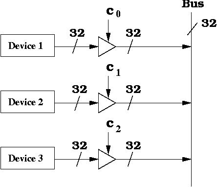
In computer architecture, a "bus" is usually some kind of "tri-state bus", also called a "3-state bus".
The datapath -- a high-level "napkin sketch" of a CPU design -- generally shows one or more buses, which often need to be 3-state.
Conceptually the simplest approach is to stick on the output of every register and every ALU a "3 state bus driver chip" that is, in turn, connected to the bus.
Any one of (in no particular order)
74HC245,
74HC640,
74HC645,
74HC7541,
74HC623,
would work.
Whenever you want data from any register or ALU,
the control logic of the machine enables the output (controlled by a pin on the 3 state driver chip often labeled "/OE") of the corresponding bus driver, and disables the output of all the other bus drivers connected to that bus.
Then anyone reading data from the bus sees the data from the selected register or ALU.
Typically all the "/OE" pins are all driven by a single "selector" chip designed so that at most one output is ever driven active -- such as a 74HC137 (which stores 3 bits of your instruction register) or a 74HC138 (which requires 3 bits presumably stored in an instruction register elsewhere).
With this approach, you could implement a single-read-port 32-bit register file of 4 registers with a 74HC273 plus a bus driver chips per every 8 bits stored, plus a selector chip -- a total of 33 chips.
You could implement a 2-read-port 32-bit register file of 4 registers with a 74HC273 per every 8 bits stored, with 2 bus driver chips per 74HC273 -- one bus driver for each read port -- plus two selector chips, one per read port -- a total of 50 chips.
(But see below for ways of building a functionally-equivalent 32-bit x 4 register file with fewer chips).
the register file
As supercat pointed out, you can design a functionally equivalent system in fewer chips by using chips with 3-state drivers built-in.
In particular, many 8-bit register chips have tri-state outputs, so their "output" pins can be directly connected to the bus, even though other chips also have their "output" pins connected to the same bus --
such as (in no particular order) the 74FCT574, 74HCT574, 74HC646, 74HC652, 74AC534, or a 74HC374.
For example, you could implement a single-read-port 32-bit register file of 4 registers using 16 octal tri-state register chips plus a selector chip.
A 2-read-port 32-bit register file of 4 registers would require 34 chips.
A single-read-port 32-bit register file of 4 registers using the 74HC670 3-state 4x4 register files requires 8 chips (the selector and the 3-state bus driver is built into this chip).
A 2-read-port 32-bit register file of 4 registers using the 74HC670 3-state 4x4 register files requires 16 chips.
There exist single chips, such as a 74HC7403 or a 74HC7030, that can store more bits than an entire 32-bit register file of 4 registers, and have 3-state outputs to easily interface to a bus, but I haven't yet figured out a good way to use them in a register file.
general comments
For concreteness, I named specific chips from the 74HC family.
Functionally equivalent chips (with the same part number, except the different family letters in the middle) are often available in TTL -- in the 74LS, 74F, etc. families -- and in CMOS -- in the 74HC, 74AHC, 74HCT, CD4000, etc. families.
A CPU built entirely of such CMOS chips or TTL chips (from any of the above families) is often called a "TTL CPU", for lack of a better name.
I encourage you to post your partially-completed CPU design online,
and ask daveb to add you to his Homebuilt CPUs WebRing -- see the instructions at the bottom of Simplex-III, daveb's homebuilt CPU.
Perhaps you might be interested in picking up some tips and tricks from other people who have succeeded in building TTL computers:
- the book "Computer Architecture" by Hennessy and Patterson (often alluded to as "H&P"). The main part of the book talks about a lot of complicated stuff that's not really relevant to people building a TTL CPU -- but there's a great appendix that explains in detail how to build one particular TTL CPU. In particular, it gives some good tips on how to build a register file out of off-the-shelf TTL chips.
- the Homebuilt CPUs WebRing mentioned above
- Wikibooks: Microprocessor Design: TTL CPUs
As you can see by browsing the above links, most Homebuilt CPUs are "TTL CPUs" built out of SSI/MSI TTL or CMOS chips, but there are a few notable exceptions.
trying to stick with fixed size instructions
Great. I encourage you to stick with fixed-alignment, fixed-width instructions on your first machine -- it avoids many quirky issues with non-aligned instructions -- or worse, variable-width instructions.
8 bits is hard to work with
because it means I have to squeeze in control bits plus an immediate
address argument for the instruction into only 8 bits, severely
limiting my address space
Huh?
Lots of processors have 32-bit instructions and relatively large address spaces, and yet somehow manage to run code stored in 8-bit-wide program memory.
The 8088 uses instructions occasionally 32 bits or longer, connected to 8 bit memory.
The (non-Thumb) Arm processors use instructions always 32 bits long, often connected to a 16-bit memory, and occasionally 8-bit boot ROM using the BOOT8BIT bit.
The 68008 uses instructions at least 16 bits long, occasionally 32 bits or longer, connected to 8 bit memory with a 22 bit address bus.

