3
\$\begingroup\$

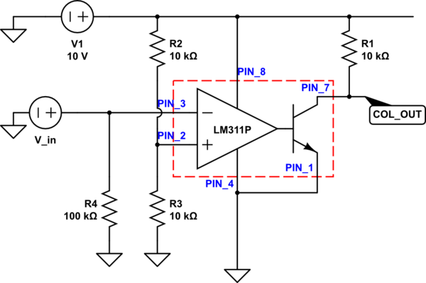
I'm implementing the comparator circuit below, with the LM311P IC.

I changed V_in's voltage from 0 to 9, making it above and below the 10/2 = 5V threshold at the V+ input. I was expecting that whenever V_ < 5V, the output to be L, and the output to be H otherwise.

However, the output of the comparator is never changing. The output is 1.43V either V_in is 3V or 8V. I checked with a voltímeter every input and checked that the input voltage differences were correct.

I've tried with 2 different LM311P and none of them worked for this circuit!

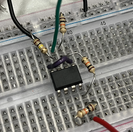
I also included a photo of the circuit: green wire is V_in (2 or 8V), red wire is Vcc (10V), black wire is ground for both voltage sources.

schematic

simulate this circuit – Schematic created using CircuitLab

enter image description here

\$\endgroup\$
7
  • \$\begingroup\$ That circuit could be damaging the chip. The chip is probably designed to connect pin 7 to Vcc and put the load between pin 1 and GND. At the moment, there is no element to limit the current going out of the opamp, to the base of the transistor to GND! \$\endgroup\$
    – Saadat
    Commented Feb 12 at 16:52
  • \$\begingroup\$ @Saadat but PIN_1 is EMIT_OUT. From the schematics I saw, EMIT_OUT should be grounded. At least that's what I understand from the datasheet \$\endgroup\$
    – ludicrous
    Commented Feb 12 at 16:57
  • 3
    \$\begingroup\$ There's nothing wrong with grounding the emitter, it's left open so (for example) you could ground it when using split supplies or use it to drive a load. I don't see anything wrong with your circuit except for the lack of supply decoupling, so double-check your experimental setup, probe all the node voltages for each state (when you expect the output to be low, then high). That should provide enough information to see where the problem is. \$\endgroup\$
    – John D
    Commented Feb 12 at 17:12
  • \$\begingroup\$ Is there a connection between the blue GND bar and pin 4? \$\endgroup\$
    – Jens
    Commented Feb 12 at 19:12
  • 1
    \$\begingroup\$ Are you sure that it is a 'real' LM311? -> electronics.stackexchange.com/a/687184/343715 \$\endgroup\$
    – Gos
    Commented Feb 12 at 19:26

1 Answer 1

0
\$\begingroup\$

What you've put together is an inverting comparator circuit.

So which signals are you trying to compare? It looks to me like whatever's going into V_in is being inverted by the inverting input (-, pin_3), while your non-inverting input (+, pin_2) is getting fed 5V from V1 through the voltage divider.
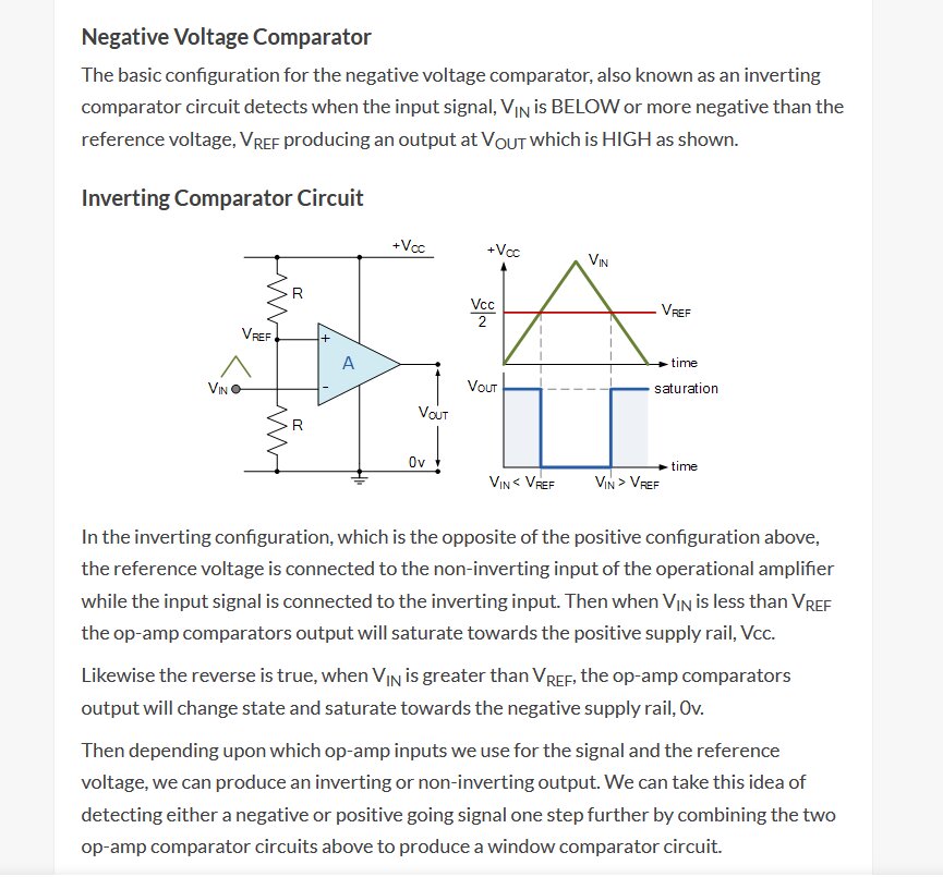
inverting_comparator

Your reference voltage is the voltage-divided 5V, and your V_in, between 2-8 or 0-9V, is always going to be "less than" V_ref because the inverting input inverts whatever value you put into it. +ve voltages become -ve, -ve become +ve, so the op-amp is saturating towards the negative rail of the chip, which in your case, is ground, and so it rests around 1.43V because of losses/gains throughout the circuit's componentry (theoretically, you'd see "0V", but that's not the real-word state of the component's materials).

Whatever goes into the inverting input, in your case, 3V or 8V, is going to be -3V or -8V to the op-amp in the LM311. Whatever inverted voltage on pin 3 is what'll be compared against whatever's going into the non-inverting input, in your case, only 5V.

From the datasheet:

"A typical LMx11 application compares a single signal to a reference or two signals against each other. Many users take advantage of the open-drain output to drive the comparison logic output to a logic voltage level to an MCU or logic device. The wide supply range and high voltage capability makes LMx11 optimal for level shifting to a higher or lower voltage."

and...

"The LMx11 operates solely as a voltage comparator, comparing the differential voltage between the positive and negative pins and outputting a logic low or high impedance (logic high with pullup) based on the input differential polarity."

To be clear, when it's talking about the positive and negative pins, it means the non-inverting and inverting inputs, + and -, not the positive and negative supply voltages (Vcc+ and Vcc-).

This is something characteristic of most chips that involve op-amps, that is, the range between Vcc+ and Vcc-, what the datasheet refers to as "input common mode voltage range". Since you're grounding the negative supply voltage pin, you're reducing the range with which you can compare your inputs on the inverting or non-inverting pins.
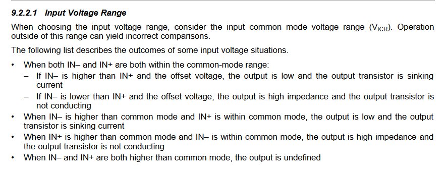
comparator voltage range

(For reference, it recommends -14.5V at most and at least 13V for lower and upper range limits, respectively. And on that note, when in doubt, dig into the datasheet. There are almost always test circuits for applications the component can be used for.)
\$\endgroup\$
3
  • 1
    \$\begingroup\$ I do not agree here: "Whatever goes into the inverting input, in your case, 3V or 8V, is going to be -3V or -8V to the op-amp in the LM311". This is not true, the schematic and the expected behavior is correct. \$\endgroup\$
    – Jens
    Commented Feb 12 at 19:07
  • \$\begingroup\$ @Jens Then you're misunderstanding what I meant. \$\endgroup\$ Commented Feb 13 at 6:27
  • \$\begingroup\$ As I understand, you state, that the comparator will interpret the given full input range of V_IN as being below the 5 V reference. This is not true. \$\endgroup\$
    – Jens
    Commented Feb 14 at 2:54

Your Answer

By clicking “Post Your Answer”, you agree to our terms of service and acknowledge you have read our privacy policy.

Not the answer you're looking for? Browse other questions tagged or ask your own question.