1
\$\begingroup\$

I'm trying to understand the schematic of this Adafruit UV sensor:

(Note: [U2] GUVA-S125D is a photodiode.) Schematic
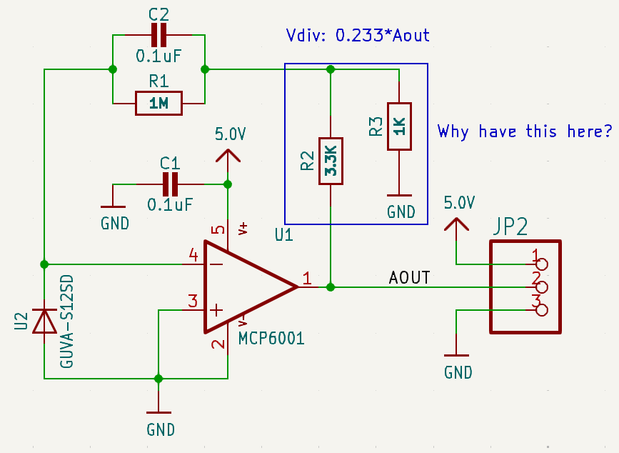
I understand the purpose of the other components, but haven't encountered a voltage divider on the op-amp feedback like this. Per the product description, the output is nominal 4.3 V, and increases proportional to the photodiode current in μA. Is the voltage divider what creates this offset? Why not have it start near zero?

\$\endgroup\$

1 Answer 1

3
\$\begingroup\$

The output voltage is nominally 0V (dark) and reaches 4.3V when the PD current is 1uA, according to the supplier.

4.3V gives you a feedback voltage of 1V at the RHS of the 1M resistor, and therefore a current of 1uA to null out the PD voltage (which is trying to go negative).

The divider allows a lower value feedback resistor (1MΩ rather than 4.3MΩ) and a higher value of feedback capacitor (100nF rather than 23nF) and there's not a lot of else different for this application. Possibly more (or entirely) parts they always keep mounted on feeders on their P&P machine.

\$\endgroup\$

Your Answer

By clicking “Post Your Answer”, you agree to our terms of service and acknowledge you have read our privacy policy.

Not the answer you're looking for? Browse other questions tagged or ask your own question.