2
\$\begingroup\$

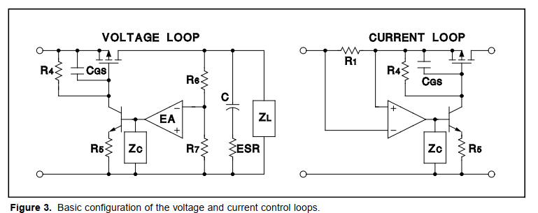
I recently came across this figure detailing the compensation of the UC3833 in the App Note “A High Performance Linear Regulator For Low Dropout Applications” Available here and they show the use of both a current loop and a voltage loop for compensation.

LDO using double compensation loop

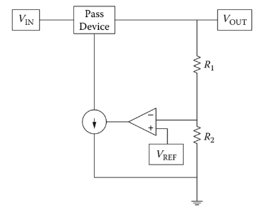
I am familiar with the use of only one loop, namely a voltage loop for compensation like shown in this figure (taken from chapter 5 of “DC Power Supplies” of N. Kularatna)

LDO using a single compensation loop

So now my question is why is the additional current loop necessary or advantageous? Any link to background information is greatly appreciated

\$\endgroup\$
0

2 Answers 2

2
\$\begingroup\$

why is the additional current loop necessary or advantageous?

The UC3833 data sheet is helpful about this: -

Additionally, they feature an innovative duty-ratio current limiting technique
which provides peak load capability while limiting the average power dissipation 
of the external pass transistor during fault conditions

It doesn't play a role in compensation.

\$\endgroup\$
0
2
\$\begingroup\$

The left circuit is a closed loop to regulate the voltage at the output, which you say you already understand.

This regulation has nothing to do with compensation.

The circuit on the right is another, different closed loop, limiting output current. That current has to pass via R1, which will develop a potential difference across it proportional to current through it, according to Ohm's law. The differential amplifier measures that potential difference, and its output (with the help of a BJT) is used to control the gate of the MOSFET. In this way when current reaches some maximum permissible value, the MOSFET is switched off to some extent, preventing current from rising any further.

None of that has anything to do with compensation either.

I believe what you meant to say was "they show the use of a current loop and a voltage loop, both of which require frequency compensation". Higher frequency components of the changing currents and voltages may (and will) undergo phase shifts on their way around the loop, and if that phase shift is significant enough, what should be negative feedback becomes positive, with consequences such as ringing or even oscillation.

To prevent this, phase shift is corrected or compensated for by altering feedback amplitude at higher frequencies (or in other ways), a task performed by the blocks labelled "Zc".

\$\endgroup\$
1
  • \$\begingroup\$ Thanks Simon, yes I misused the term "compensation" in my question statement, thanks for the clarification and explanation of the function of both feedback loops \$\endgroup\$
    – Ken Grimes
    Commented Aug 30 at 18:26

Your Answer

By clicking “Post Your Answer”, you agree to our terms of service and acknowledge you have read our privacy policy.

Not the answer you're looking for? Browse other questions tagged or ask your own question.