1
\$\begingroup\$

Recently, I have been working on a circuit that requires an input voltage range of 28-33VDC, with the output voltage consistently maintained between 28-30VDC. I referenced circuit from the following link:

https://www.eetimes.com/clamping-circuit-tames-automotive-voltage-transients/

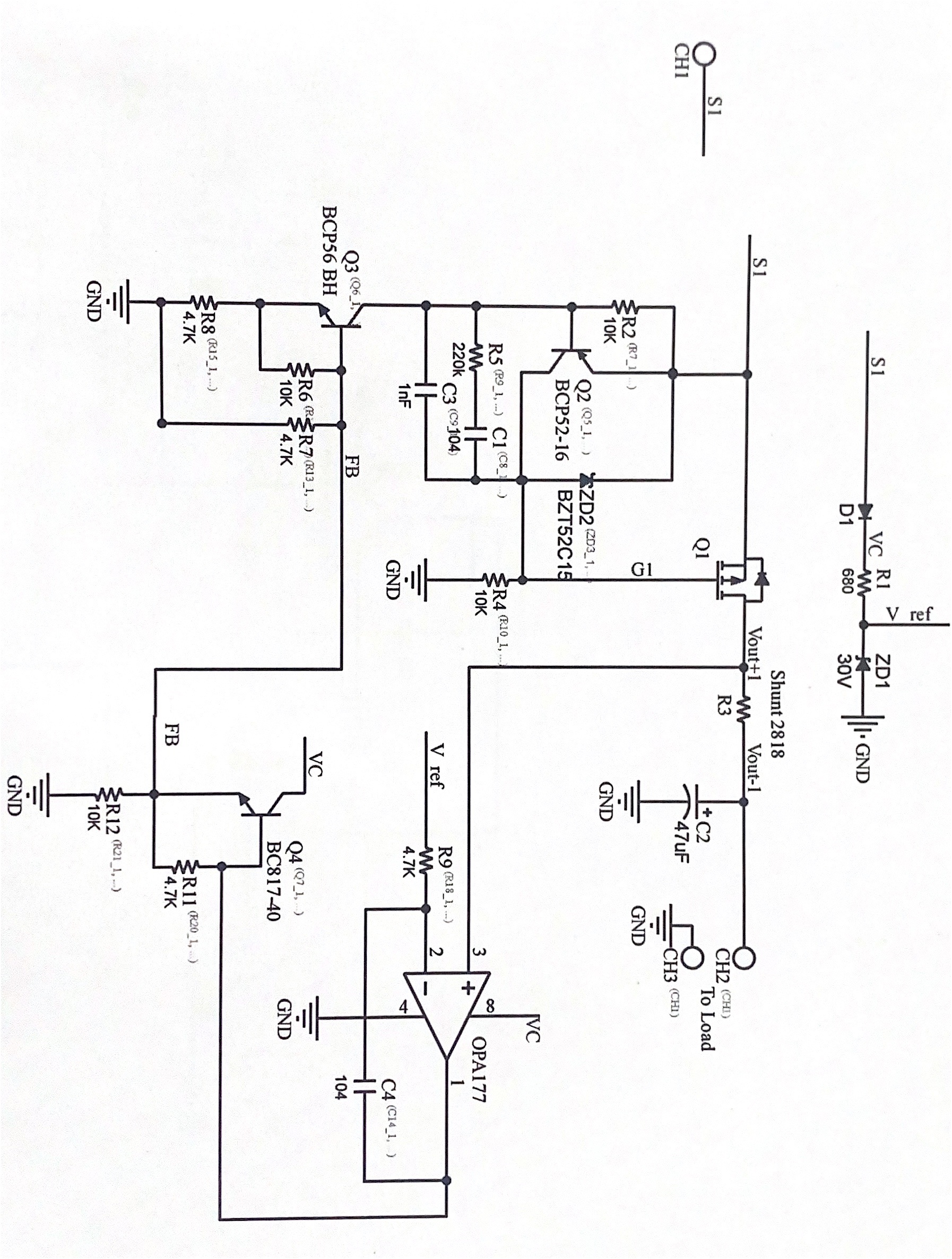
Instead of using a Zener diode at the output, I designed a voltage feedback loop using an op-amp (the schematic is attached below). Here are the results of this circuit:

  • No Load Condition: With an input voltage ranging from 30.5-33V, the output voltage performs well, clamping at 30V with no ripple, when the input voltage is below 30V, the output voltage changes according to the input voltage without clamping. However, unfortunately, in the range of 30-30.5V input, the output voltage exhibits ripple (upto 700mV pk-pk).
  • Loaded Condition (>3A): Similar to the no-load condition, but the region where ripple occurs is larger (from 30-31V input).

I have tried changing the values of the output capacitor and the compensation capacitors, but the situation has not improved significantly.

Could anyone spare some time to help me?

Thanksenter image description here
\$\endgroup\$
6
  • \$\begingroup\$ Welcome! What's your reference voltage set to in your regulator? \$\endgroup\$
    – winny
    Commented Nov 5 at 8:59
  • \$\begingroup\$ The reference voltage is set to about 30V. It is created using a 30V Zener as shown at the top of the figure \$\endgroup\$ Commented Nov 5 at 9:03
  • \$\begingroup\$ What were your reasons for changing the design and have you used a simulator? \$\endgroup\$
    – Andy aka
    Commented Nov 5 at 9:07
  • \$\begingroup\$ If you have 30 V DC in with +-700 mV, the regulator set to 30 V won't have any possibility to regulate away the bottom part of your ripple. You need voltage margin in any linear regulator design. \$\endgroup\$
    – winny
    Commented Nov 5 at 9:13
  • \$\begingroup\$ R9 and C4 severely limit the slew rate of the op-amp, which (at first glance) will spend a lot of time with output railed near 0V. I suspect it can't change/rise fast enough to prevent output overshoot. What frequency of errant ripple are you seeing? Also, why did you employ the op-amp, and not go with Betten's original design? \$\endgroup\$ Commented Nov 5 at 10:32

1 Answer 1

1
\$\begingroup\$

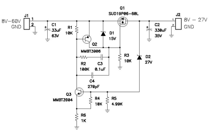
I can see that the original design would work (given also that I've designed similar circuits previously): -

enter image description here

As soon as the output voltage rises too high it begins to turn on Q3 and, when that happens, Q2 also begins to activate thus Q1 (the pass MOSFET) is nudged into saturation and it limits the output voltage. In other words it acts as a linear regulator.

The likely main problem with your circuit is down to the poor choice of op-amp. For a start it doesn't have rail-to-rail inputs and, when the operating point is reached, the op-amp won't necessarily behave how you expect it to. It also looks like that the non-inverting input could be up to 0.7 volts higher than the power rail for the op-amp.

This is due to D1 in your design that drops the incoming supply by one diode drop before feeding the op-amp positive rail. There is no margin in the data sheet for this and, you will exceed the absolute maximum limits for the op-amp.

The op-amp hasn't got rail-to-rail output capability either and that could easily mean that Q3 won't be turned off properly. It's all a bit hit-and-miss.

Added to this is the massive gain increase when you introduced the op-amp circuit. I fully expect that this massive gain increase is going to give stability issues (if and when you sort out the issues listed above). Maybe that's what you are seeing when you say this: -

the output voltage exhibits ripple (up to 700mV pk-pk)

\$\endgroup\$

Your Answer

By clicking “Post Your Answer”, you agree to our terms of service and acknowledge you have read our privacy policy.

Not the answer you're looking for? Browse other questions tagged or ask your own question.