4
\$\begingroup\$

I use Eagle Cad 6.4 to prepare PCB layouts then manufacture them at home. As I use amateurish equipment and method, I would like to have bigger pads as much as possible so that when I drill the pad holes, I will have a very large ring of copper around the hole to solder. It would be convenient to have bigger pads (when it is possible on the layout). I can do it on photoshop for sure or maybe by redefining each component's packet description on the library, but it is a little bit time consuming. I wonder if there is an easy tool like change tool to enlarge the pads I want.

The pads I'd like to enlarge are the green circles below image. For example, the diode (the most left circle ) has a bigger pad area, where as the resistors (the closest two green circles) have thinner circles.

enter image description here

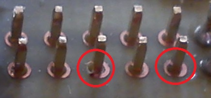
When I drill these holes, sometime the drill takes the copper away and I'm left with rings that are too thin. For example, please see the below photo. These pins are not important but in some cases, it would be better to have a larger copper area. Is it possible to do it on Eagle Cad 6.4? enter image description here
\$\endgroup\$
5
  • \$\begingroup\$ You can't set the thickness in Eagle. Even if you could, it would not be for individual pads but for the board, or at least that layer, as a whole. You tell the board house you want "1oz copper", "2oz copper", or whatever. In your case it depends on the copper thickness of the stock you get. \$\endgroup\$ Commented Jul 7, 2013 at 16:22
  • \$\begingroup\$ Now you are really confusing things. It appears you mean the diameter of the pads, but you explicitly say you do NOT mean the diameter of the pads. Giving up. \$\endgroup\$ Commented Jul 7, 2013 at 17:18
  • \$\begingroup\$ The pad (green circles) are made of traces. 0.6 mm or 3.5 mm diameter drill radius would not enlarge thickness of the trace, the thickness is the same. I want to enlarge the thickness of the trace that creates the green circle. Therefore I do NOT mean the diameter. I hope it is clear now? \$\endgroup\$
    – Angs
    Commented Jul 7, 2013 at 17:25
  • \$\begingroup\$ No, you DO mean the diameter of the pad. And again, this has nothing to do with the thickness of the copper. The first time I can attribute to unfamiliarity with English, but if you keep doing it after this was explained to you then it's just wrong. Do a HELP DIAMETER in Eagle. \$\endgroup\$ Commented Jul 7, 2013 at 19:31
  • \$\begingroup\$ Pads are drawn by the CAD software as a circle, with a hole in the middle. It's not a circular trace, so you're thinking about the mechanics of making the pad larger incorrectly. \$\endgroup\$ Commented Jul 7, 2013 at 21:12

2 Answers 2

5
\$\begingroup\$

EAGLE has no say over the outcome of the thickness of the actual copper layers themselves, since you'll be etching the board yourself and you're the one picking the copper board stock. However, you can increase the size of the annular ring to give yourself more room to drill a hole close to the center of a PTH.

Using the Info tool (the button that is the letter i), click on the PTH you are interested in and adjust the Diameter from auto to another value that is greater than your Drill size. Click Apply and visually inspect the hole - if it's still not as much copper as you want, increase the Diameter again until it's as thick as you want.

If you want to do this to all your PTHs, just use the Change tool, go to Diameter, and click the ... option at thebottom to set a custom value. This would ideally be the Diameter you chose when playing around with a single PTH. Then just start clicking on the other PTHs you want to update them.

This will only work, however, on PTHs you defined manually on the board layout. If some PTHs are part of the part's package, for example, you will have to edit their Diameter manually in the package itself, not in the board layout.

\$\endgroup\$
11
\$\begingroup\$

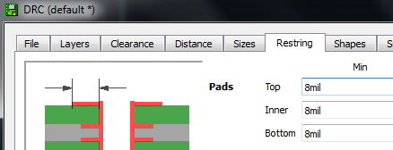
To have a minimum annular ring at pads, open your DRC in the PCB window, go to the RESTRING tab and set there the minimum for your pads in top, bottom (I guess you are not using inner layers). For my experience with DIY pcbs, a value over 12 mils works. Note: take care as this can create pad-to-pad clearance violations.

enter image description here

\$\endgroup\$

Your Answer

By clicking “Post Your Answer”, you agree to our terms of service and acknowledge you have read our privacy policy.

Not the answer you're looking for? Browse other questions tagged or ask your own question.