8
\$\begingroup\$

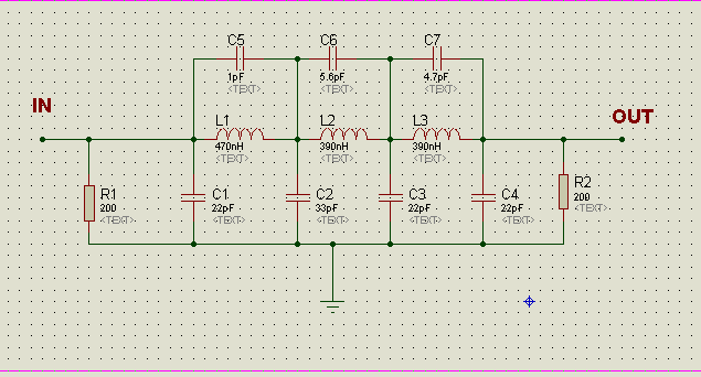
I have designed a FPGA based DDS and now I want to add a low pass filter to its output. Previously I was working on a project based on AD9850 DDS(0-50MHz) and I had a commercial module for it that had a low pass RLC filter which worked excellent ( schematic below). Now I want to use the same design for my own frequency (fc= 70,100 ,120 MHz with different setups) but I can not analyze its values.

I think R1 and R2 serve as parts of two back-to-back RLC+LCR filters (something like designs in rows 3,5 here ) but I don't know what those small capacitors C5-C7 are doing there? .

I also don't know why L1 inductance differs from L2,L3 (From answer of Andy Aka in this thread I just can guess it is related to the impedance between steps but can't realize how to calculate them? )

I am looking for a formula or method for calculating these values ( R1,2 C1-C7, L1-L3) for other frequencies ( for example for fc=70, 90, 100, 110 ,.. MHz).

For example assume we have fc=100MHz. How do you select part values in this design?

enter image description here

\$\endgroup\$
4
  • \$\begingroup\$ I can't help with the specifics of this filter but you might like to look at Elsie, the electronic filter design software. \$\endgroup\$
    – David
    Commented Nov 11, 2013 at 8:42
  • \$\begingroup\$ @David I looked at it. Is it free? \$\endgroup\$
    – Aug
    Commented Nov 11, 2013 at 8:45
  • \$\begingroup\$ Yes, for student/hobbyist use it is free up to 7 stage filters. For professional use with larger filters you will need to purchase a key. I don't know if they specify non-commercial without a key, you'll have to check the license. \$\endgroup\$
    – David
    Commented Nov 11, 2013 at 8:48
  • 1
    \$\begingroup\$ have you tried doing some s-domain analysis? obtaining the transfer function of the filter may help a great deal determining the component values in relation to filter characteristics. \$\endgroup\$
    – deadude
    Commented Nov 11, 2013 at 23:10

5 Answers 5

5
+50
\$\begingroup\$

The classic answer to this question must be "Zverev". But that might be overkill, unless you have access to a really good library.

A simpler and non-mathematical answer to some of your questions is possible, which may help:

R1 and R2 provide impedance matching; the original filter is designed to accept a signal driven from a specific source impedance, and deliver its output to a specific load impedance (R1,R2 are also mentioned later). These impedances are:

  • normally the same
  • known as the "characteristic impedance" of the circuit
  • usually the same as the characteristic impedance of the application's standard cables (e.g. coaxial cable in RF applications)
  • commonly (but not always) 50 ohms. (you will see 75 ohms in video applications, and (rarely nowadays) 600 ohms in audio and telephony.

Check the original filter info for its characteristic impedance, but 50 ohms is most likely. So - the impedance of the L-C network was not exactly 50 ohms, and R1,R2 reduced the input and output impedances to match.

C5,C6,C7 ... Consider that C5 and L1 on their own form a parallel L/C resonant circuit. This acts as an inductor (L1) at low frequencies, and as a pure capacitor at high frequencies (VERY high since it is 1 pf!)

But at the resonant frequency, the impedance is infinite. Therefore at this frequency, the filter will have infinite attenuation. (Over-simplification! all the components interact with each other, so the actual frequency is slightly different from this calculation)

There are three such notches in the frequency response; and you can learn a bit about this filter by calculating C5/L1, C6/L2, C7/L3. Usually 2 are quite close together and the third will be significantly higher; without doing the math I can already see that here.

That makes this a 7th order Cauer filter (or Cauer/Chebyshev) and the art of getting good stopband rejection (or the reason for 592 pages of Zverev) is the art of tuning C5-C7 to place those notches (last picture on Wiki page) the right distance apart so the peaks between them are all the same height.

Theory apart, circuit tolerances virtually guarantee tweaking trimmer caps or inductor cores while watching a spectrum analyzer for best results!

C1 to C4 also resonate with L1 to L3; in this case, the main effect is on the passband flatness as well as the actual cutoff frequency (which must be below the first notch!) It can be understood as a cascade of 2nd-order sections with different characteristics and one first-order section. Look at Figure 3 in that article (embedded below, hope that's OK)
enter image description here

It shows underdamped sections (with peaks) and overdamped ones (which just roll off). A skilful combination of these will give an (approximately) flat response up to the cutoff. Again, I cannot cover the details here, but I hope it is clear how different values of inductor forming different 2nd-order filters are part of the puzzle. Getting R1 and R2 wrong will principally affect the passband flatness, by affecting the Q (damping) of the input and output sections (L1 etc and L3 etc).

Here is a more typically mathematical explanation

Now to the most important part of the question:

How do I select part values for 100 MHz?

Given all the above, usually not from scratch... You can take an existing filter, and simply scale it.

Given Xl=jwL and Xc=1/jwC,
assuming the current filter is set for 50MHz,
assuming you want the new filter set for 100 MHz
and assuming the characteristic impedance is to remain the same,

you can simply halve all the inductances and capacitances, so that Xl is the same at twice the frequency, and ditto for Xc. Resistances remain the same, since the characteristic impedance is the same, and a resistor's impedance is not a function of frequency. (Check both versions in simulation!)

\$\endgroup\$
2
  • \$\begingroup\$ Thank you very very much for such nice explanation! I really learned a lot from this answer but I have a bit confusion with the last part: "scaling the filter". It was the first thing I thought about. All the scalings work nice only on the paper! Practically I received sub-optimal results by this method. I think I need designing a Cauer or M-derived or Constant-K family from the scratch but don't know which one is easiest to design. BTW your answer is a complete one. \$\endgroup\$
    – Aug
    Commented Nov 16, 2013 at 23:08
  • 1
    \$\begingroup\$ If the scalings also work in simulation but not real wire, then parasitic components are getting in the way. (You may have more than 0.5pf stray capacitance!) The original filter may have been very carefully laid out on PCB, perhaps with tricks to neutralise stray components : there is a LOT of practice involved and as a young engineer I had some dismal failures at it. Now there are specialist RF filter design tools but I am the wrong person to describe them. \$\endgroup\$
    – user16324
    Commented Nov 16, 2013 at 23:26
4
\$\begingroup\$

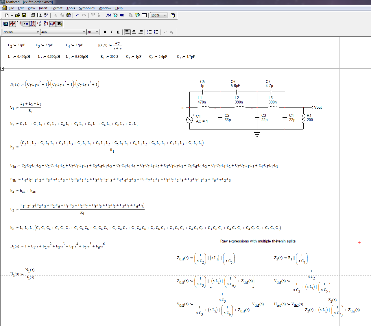
This filter features 9 energy-storage elements but you can see that when the excitation voltage \$V_{in}\$ reduces to 0 V, \$C_5\$ comes in // with \$C_2\$ and you lose an order. Then, if you further observe the other capacitors, like \$C_2\$, \$C_6\$ and \$C_3\$, they form a capacitive mesh whose states variables are not independent. Same for \$C_3\$, \$C_7\$ and \$C_4\$. You lose two more orders. As a result, the denominator \$D(s)\$ is of degree 6. For the numerator, we can apply the fast analytical techniques or FACTs immediately. If the associations of \$C_5||L_1\$ or \$C_6||L_2\$ or \$C_7||L_3\$ become transformed opens, you have zeros. Therefore, the poles of each of these resonating network become the zeros of the transfer function. We can therefore immediately express the numerator \$N(s)\$ without writing a line of algebra, just a quick impedance calculation:

\$N(s)=(1+s^2C_5L_1)(1+s^2C_6L_2)(1+s^2C_7L_3)\$

The dc gain of this circuit is 1, then the transfer function is given by:

\$H(s)=\frac{(1+s^2C_5L_1)(1+s^2C_6L_2)(1+s^2C_7L_3)}{1+b_1s+b_2s^2+b_3s^3+b_4s^4+b_5s^5+b_6s^6}\$

To determine all these coefficients, you can either go for the FACTs or use Thévenin and rearrange quickly with Mathcad. This is what I did and the result appears in a well-ordered form below:

enter image description here

Then you can check how the Thévenin expression compares with the low-entropy form. Of course, further arrangement are possible in the denominator to form more compact canonical forms but the whole expression is correct.

enter image description here

FACTs are truly the way to go to analyze any type of transfer function. Sometimes you can combine them with a more classical approach as I did here but you always save time. You can discover an introduction to FACTs here http://cbasso.pagesperso-orange.fr/Downloads/PPTs/Chris%20Basso%20APEC%20seminar%202016.pdf

\$\endgroup\$
2
\$\begingroup\$

I cannot give you a fixed formula to design your filter, because it all depends on what exactly you want from it. You are essentially looking at an optimization problem that includes much more than just a corner frequency.

If you cannot be bothered with additional details, you could just try this dumb hack: Scale all values to get to your desired frequency. Ignoring the small capacitors C5 through C7, the circuit you have drawn is a multi-pole low-pass filter with a corner frequency around 50 MHz. To go to 100 MHz = 2 * 50 MHz, divide the values of all capacitors and inductors by 2. This approach will shift the corner frequency without changing the impedance (at the corner frequency). So watch out if the impedance that matters to you is defined at a frequency that does not scale the same way as the corner frequency!

If you do want to improve your chances of getting a particularly good result, you will need to understand the requirements you have (or the problems this circuit solves). For example, one effect of slightly spreading the individual resonance frequencies (L1 * C1 != L2 * C2, ...) is smoothing out the frequency response around the corner. Another affected characteristic that may or may not matter for you is signal dispersion and related quantities (phase shifts, delay time), etc. If you choose nominally identical values, some of these end up essentially undefined at the corner frequency because they may depend extremely sensitively on component variations. Spacing resonance frequencies by what corresponds to slightly more than component tolerances hence helps you in reliably getting at least qualitatively the same behavior from nominally identical circuits. But this may not matter in your application.

I think you should at least try to figure out what C5 to C7 do. My best guess is that they shift an internal resonance of L1 to L3 out of a frequency band that matters for the application. If you either change the inductors or the frequency range you wish to use the circuit in, you may have to adjust these accordingly. And in a different way if they serve a different purpose---after all, it just might be that my guess of their purpose is wrong and they instead should flatten the frequency response in some range or compensate some undesired phase shift...

\$\endgroup\$
1
  • \$\begingroup\$ If you want to go into more depth with filter design, have a look at some tutorial. This one looks promising, but I am sure there must be lots of good ones out there. \$\endgroup\$
    – user30985
    Commented Nov 13, 2013 at 12:19
1
\$\begingroup\$

Basic Stuff

1: Clock Filtering

DDS generators work at a constant clock rate, with a [programmable] phase increment between samples. The main point of the filter is - to remove that clock.

2: Reduce Noise / Distortion

The practical limit of a DDS is less than 1/2 the clock rate. The closer you get to 1/2, the worse the signal gets. A better limit is 2.5 or even 3 (ie. 1/3 of clock rate)

3: Summary- change the clock = change filter parameters If you design a filter for Fc=70MHz, it will still work for Fc=120MHz. You'll just be filtering out a whole load of frequencies that would have been ok.

I'd suggest finding the highest clock frequency that works with you FPGA, then stick with it. This will give you the widest range of output frequencies, and simplify the filter design.

Filter Part Selection

On to the good stuff! Filters can be analysed in Excel if you know circuit theory. There are whole books on this topic, so I'm going to limit myself to your questions.

R1, R2 = Source & Load impedance If you started out with AD9850, you may be aware there's a limit how much current it can provide. There's a similar limit on the currents out of your FPGA, and we haven't even discussed what DAC (Digital to Analog Converter) you are using.

L1 is different

Plenty of ways of looking at this. Chebyshev filters (for example) almost never have the same values. Or you could just think of L1 doing the "heavy lifting" because it's the first inductor to get the signal.

C5-C7 help block the clock

A capacitor in parallel with an inductor form a "tuned circuit" at a particular frequency (like tuning a radio). Picking the right values here will help block your sample clock. Changing the sample clock rate, as you suggest, makes these less effective.

In Conclusion

If you really want to play with filter design, it's a heck of a lot easier to download and use a program. In this instance, the program I use is from Iowa Hills Software and is called RF Filters (they do digital filter designs, too)

\$\endgroup\$
0
\$\begingroup\$

I'm sorry for the necromancy, and I apologize for some of the tone I may be using, but I can't agree with many of the points in the answers. I'll leave the critiques at the end. I the meantime, I'll try to address OP's problem, as stated.

OP, what you have there is a passive filter. The sin of these is that they need ro be recalculated everytime something changes. If the I/O impedances remain the same, or if their ratio is the same, then it's a simple matter of scaling the reactances involved. This means a simple multiplication with the ratio of the frequencies and the impedances. E.g. if your circuit needs to be shofted for 100 MHz, while changing the I/O to be 100 Ω, both, then it's a simple matter of multiplying each inductance with 70/100*100/200, and each capacitance with 70/100*200/100; overall, each. If not, you need to recalculate, and this is either done with tables (if they exist for your particular case), or calculate them, yourself.

In the latter case, you should know that this has been an art for the past 100+ years, and even today the methodologies are virtually unchanged. The usual suspects are:

a) Filter synthesis. In short, calculate the input impedance transfer function, form the H(s)H(-s), add I/O, mix in and calculate the reflection coefficients, start eliminating poles and zeroes. On the ay there you may (often) encounter cases where you won't know which pole or zero goes where, so you'll have to aplythe Hurwitz criterion to ensure that the remaining transfer function is realizable, and only then continue. If successful, you'll obtain a continuous fraction which gives you the values. Unfortunately, this method is more suited for all-pole filters (Bessel, Butterworth, Papoulis, Halpern, Chebyshev type I, etc), since the presence of the zeroes makes capacitors like your C5, C6, C7 complicate the matter. Personally, I never liked this approach, so for me it's the second:

b) Write the mesh equations, solve for the transfer function symbolically (or use FACTS, or any other method that suits you); this would be A(s). B(s) will be the target transfer function, appropriately scaled with the gain and the I/O divider -- pole-zero transfer functions for lowpass filters imply a zero is always larger, so the transfer function needs scaling with the ratio of the squared pole(s)/zero(es). Normalize to the zeroth power of the denominator and the numerator, equalize the two transfer functions, form a system of equations (polynomials, more likely), let the computer sort them out. Output: values.

I think R1 and R2 serve as parts of two back-to-back RLC+LCR filters

As others have said, those are the I/O impedances for which the filter is calculated. The presence of the shunt R1 tells that the output is a current generator. Just so you know, the filter can be calculated for Ri=∞.

what those small capacitors C5-C7 are doing there?

Those form the zeroes of the transfer function; the LC filter that you see there is a whole, a typical topology for a pole-zero filter.

I also don't know why L1 inductance differs from L2,L3

Also part of the whole: their values are as calculated. Note that the values that come out of calclations are (almost always) different. For example, the value of C1 in the 1st picture below was obtained by rounding 1.690818503277825*10^-11 to 18p.

As for the calculation, this is where you need to tell more. If you're interested in calculating these values, yourself, I've told you two methods; there may be others. But if you expect something simple as the Japanese site you linked you'll be disappointed. Passive filters are more complicated because they don't have any buffering between stages. Active filters can be split into 2nd order sections, each using an opamp, which provides enough low output impedance and high input impedance for their interconnection to not matter (not quite, usually the lowest Q comes first, there are other considerents), but here each stage sees both the next stage and the previous. Not only that, but the impedances seen by each stage are variable, since they are made of LC elements (thus not flat across frequency). I have all the respect for the people that made passive filters in the past years, and even greater for those that calculated them.

At any rate, supposing you had access to a program that calculated these things, you would need to refine your requirements: what is the passband bandwidth, what acceptable ripple, what attenuation at @fp, what is the stopband bandwidth, the attenuation @fs, since this is a Cayer filter there are 7 (seven, yes) ways to calculate it (well, an infinite ways, but they can be reduced to seven): passband optimization, stopband optimization, transition width o. w.r.t. passband and stopband, passband ripple o., stopband ripple o., and minimum Q (that I know of). In general, you have 5 base parameters: fp (passband or corner frequency), fs (stopband frequency), Ap (attenuation in the passband @fp, can be different than the ripple), As (attenuation in the stopband @fs), and N (order). For filters with ripple in the passband (Legendre, ultraspherical, Papoulis, Pascal, Chebyshev I, Cauer) usually fp is considered to be the end of the ripples, but this is not necessarily true. The only thing you said was that you need the fp to differ, but have not touched fs, Ap, As, or N. Therefore your last paragraph cannot be answered unless you give more details, including what I/O impedances you have.


The critiques.

  1. Starting with the accepted answer:

These impedances are:

  • normally the same

I can think of just as many reasons why the I/O impedances should not be the same, so there's nothing normal in this.

Check the original filter info for its characteristic impedance, but 50 ohms is most likely. So - the impedance of the L-C network was not exactly 50 ohms, and R1,R2 reduced the input and output impedances to match.

The filter was designed for a current output with equaly terminated I/O of 200 Ω. That's why R1 is shunted, and the input impedances are the same, not because they needed a reduction in value. If you plot the response you'll see that the design matches that of a 70 MHz Cauer/elliptic filter (more like 72.5) with ~0.5 dB ripple (values distort too much to tell precisely), 80 dB attenuation. Using 50 Ω I/O results in an 18 dB attenuation (instead of 6) and horrible 7.3 dB ripple.

There are three such notches in the frequency response; and you can learn a bit about this filter by calculating C5/L1, C6/L2, C7/L3. Usually 2 are quite close together and the third will be significantly higher; without doing the math I can already see that here.

There's nothing "usual" about the placement of the zeroes in any of the inverse-, or pole-zero filters (inverse Pascal, inverse Chebyshev, Cauer/elliptic) -- it's part of the mathematical transfer function that makes the said filter one of the inverse Pascal, Chebyshev, Cauer, etc. Their position is calculated, by design, and there's nothing "usual" about them except the fact that they are more and more distanced as their frequency is higher (explained below, the part about the Jacobi cosine). But the emphasized part (by me) is not true. And simply because they can be seen in the simulation does not mean that they're inherited from the mathematical transfer function -- it's because the filter is made with 10% values in mind: 22, 33, 470, 390, etc, so the values got so rounded up/down that the response is distorted. This is to be expected when building passive filters, but that's not the reason as explained. To add to this, the values in OP's picture are not exactly optimally chosen, and here's how I calculated them and rounded them for the same E24:
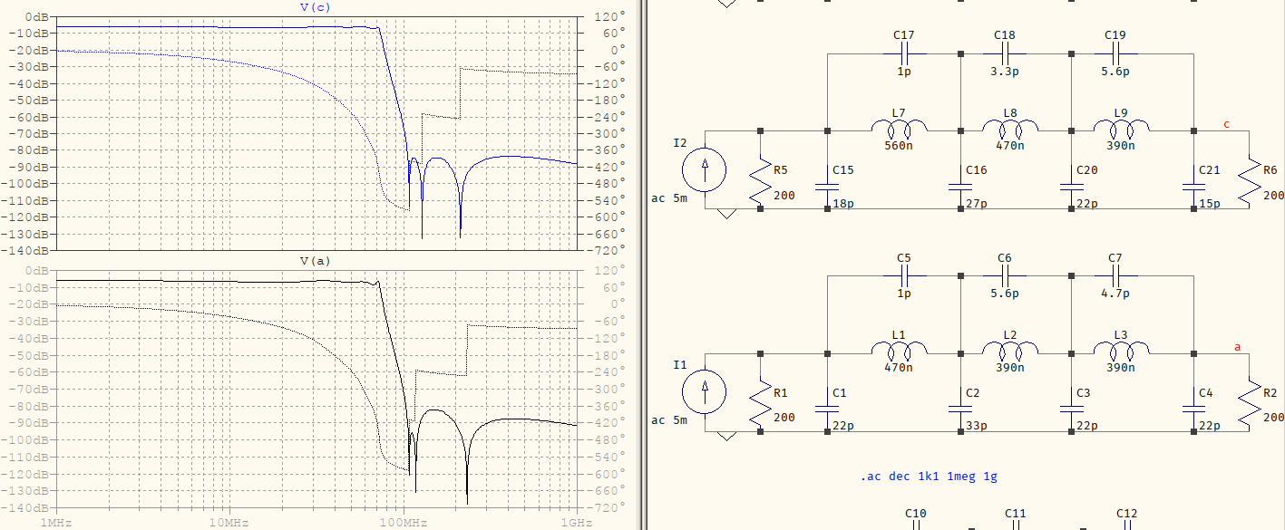
better values

I still rounded them, but look how the stopband is more equiripple than the original (which is meant to be since Cauer/elliptic means equiripple, by design), and also see how the zeroes are not necessarily "two close and one apart". They are in increasing distance, yes, since they're calculated as the inverse of the Jacobi cosine, \$1/\text{cn}(u,m)\$, similarly to inverse Chebyshev, the inverse of the cosine, \$1/\cos(u)\$. Also, the passband is more steady.

That makes this a 7th order Cauer filter (or Cauer/Chebyshev) and the art of getting good stopband rejection (or the reason for 592 pages of Zverev) is the art of tuning C5-C7 to place those notches (last picture on Wiki page) the right distance apart so the peaks between them are all the same height.

See above: they're like that by design, not by "art". The only art is in choosing the elements so that they fit the design as best as they can, given tolerances & co.

Given all the above, usually not from scratch

Again the "usual" part. The scaling can only be applied if the impedances are either exactly the same, or have the exact same ratio. If they differ, all bets are off because that's the sin of the passive filters: for ay change in the I/O (unless stated as above) you need to recalculate the elements. If the input would remain 200 Ω but the output would need to be 100 Ω, how would you distribute the difference? Linearly? Quadratically? With elliptic functions? Which ones? How? You can't. You need to recalculate everything. And Zverev is nowhere near the hard part, because you just pick the book and use the tables (if you have access to the book, sure): input four of the fp, fs, Ap, As, N, then use the tables for the particular Ri and Ro. The hard part is the recalculating. Case in point:
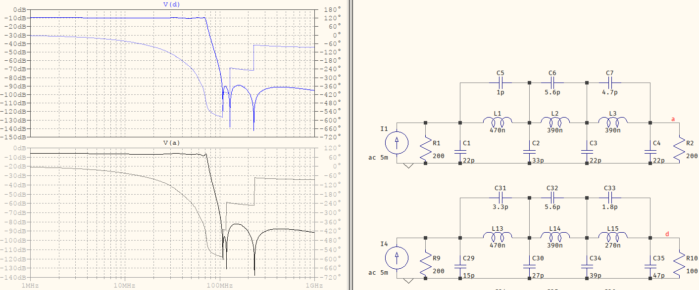
Ri=200, Ro=100

The circuit below is recalculated for the two, asymmetrical I/O mentioned above. See how it plots (blue trace). Look at the values and tell me how did you plan on getting to them? With what calculations? True, I used roundings for E24, but still.

  1. Then there's pyramids' answer, who starts in force:

I cannot give you a fixed formula to design your filter, because it all depends on what exactly you want from it.

It's a Cauer filter, so it has a precise mathematical formula, determined based on some input. Maybe you can't tell what it is, ok, but the formula can absolutely be known to very precise details. And the "what you want from it is already in the OP's first phrase:

I have designed a FPGA based DDS and now I want to add a low pass filter to its output.

Then:

You are essentially looking at an optimization problem that includes much more than just a corner frequency.

The only optimization is the Cauer filter, itself, which is the mathematically optimized filter to have equiripple. There's no other optimization involved than the formulas used for its design. Maybe I misunderstood the above quote, but there's no recursive algorithm that optimizes the response -- the Cauer filter is very much a closed form design.

I'll leave aside the 2nd paragraph since it deals with a rather brutish approach which, if you have nothing at hand, is a "good enough" approach (e.g. whatever works). But the whole 3rd paragraph seems to have been dictated by someone from PR: from "spreading the individual resonance frequencies" for the zeroes (it's a Cauer, what spreading? what smoothing?), to "signal dispersion and related quantities" (it's a Cauer, it's a fixed design; the moment you choose it you accept the Eula about its time and frequency responses), to this beauty:

If you choose nominally identical values, some of these end up essentially undefined at the corner frequency because they may depend extremely sensitively on component variations. Spacing resonance frequencies by what corresponds to slightly more than component tolerances hence helps you in reliably getting at least qualitatively the same behavior from nominally identical circuits.

Somewhere, someone from PR may be framing this as an incentive of getting better.

  1. Alan Campbell's answer is not oriented for a filter design, more of a heads-up from the DDS perspective. However, there are a few points:

If you design a filter for Fc=70MHz, it will still work for Fc=120MHz. You'll just be filtering out a whole load of frequencies that would have been ok.

While true, this is a Cauer filter, designed to be ~0.5 dB (can't really tell from the original circuit, given the not so optimally rounded values), 80 dB attenuation, which results in a transition band of roughly 40 MHz. Which means that at 120 MHz everything will be -80 dB or lower, so you can't really use a 70 MHz filter instead of a 120 MHz one (at least in this case).

L1 is different [+ paragraph]

There's no classical filter design that has the same values. Using the same values results in a simply awful response, not even lumped representations of cables or transmission lines use the same values. The only case that I can think of is the same RC filter, whose response converges towards a Gaussian, but only after many stages. It's not a practical design, more educational than not.

C5-C7 help block the clock

While that could be true, it's also not something that can be relied on since the zero is never a perfect zero, mainly due to parasitic elements (which add damping and frequency shifting), component tolerances (frequency shifting), temperature drifts (frequency shifting). So the zeroes are not for blocking the clock, they come, by design, from the Cauer transfer function. They may, or may not, help with the clock.

  1. Verbal Kint's answer is the only one that carries a good message. There is one minor point that I have to make, and that's that he uses a voltage driven filter, not current, that's why the response comes out rather distorted. But the FACTS are facts.
\$\endgroup\$

Your Answer

By clicking “Post Your Answer”, you agree to our terms of service and acknowledge you have read our privacy policy.

Not the answer you're looking for? Browse other questions tagged or ask your own question.