8
\$\begingroup\$

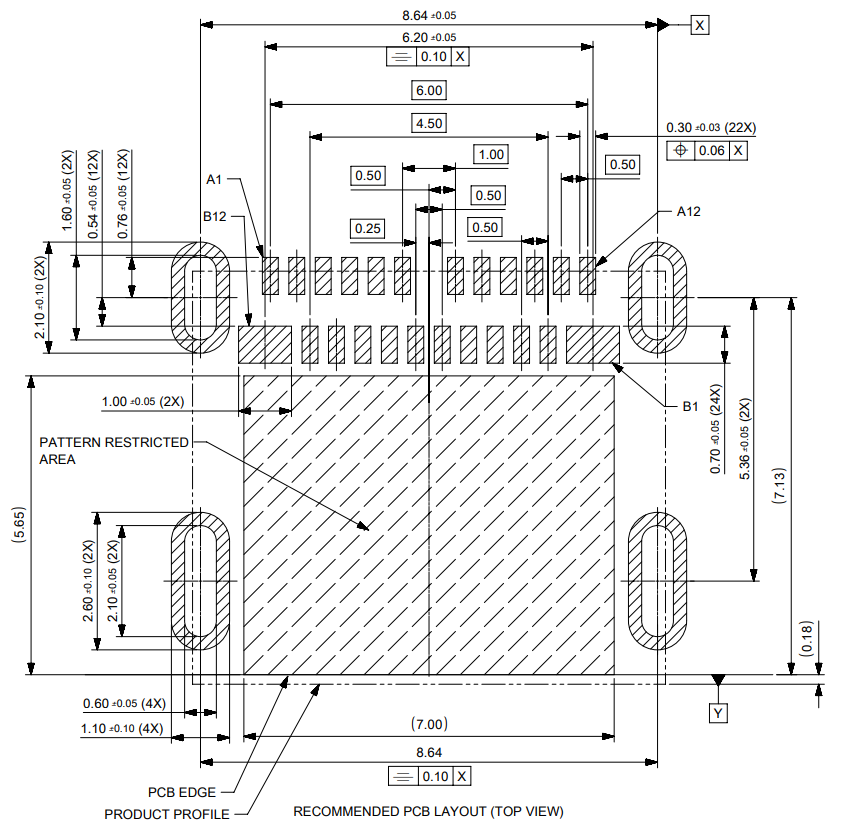
I'm having trouble understanding how to route the signals out of the Molex 1054500101 Type-C USB connector - specifically the B1-B12 pins.

enter image description here

The distance between row A and row B is only 0.5mm, too small for me to put any vias in between. That leaves me with the option of routing the B row signals away from the board into the "pattern restricted area". However if this is a pattern restricted area doesn't this mean that I am not supposed to route any copper there? I'm confused as to how to get the B row signals into the PCB

\$\endgroup\$
6
  • 1
    \$\begingroup\$ That is my understanding of 'pattern restricted area', no copper at all. I wouldn't consider soldermask covered vias acceptable, as soldermask should not ever be relied on for electrical insulation IMHO. You can certainly do vias that will fit (my current fab can do down to 0.3mm), but the cost of the board will go up. The other option is via-in-pad/active-pad. \$\endgroup\$
    – Cursorkeys
    Commented Jun 10, 2019 at 17:36
  • 1
    \$\begingroup\$ You could also break out through A1-12. I make that 0.35mm pad-pad spacing, so a 0.1mm trace will fit though and still conform to IPC spacings at USB voltages. 0.1mm traces with ~0.1mm clearance are expensive too though. Not really a lot of good options here as far as I can see. I'd probably contact Molex myself and request advice, absent advice then active-pad seems the best idea to me \$\endgroup\$
    – Cursorkeys
    Commented Jun 10, 2019 at 18:39
  • \$\begingroup\$ Maybe this will help: e2e.ti.com/support/interface/f/138/t/… \$\endgroup\$
    – EE_socal
    Commented Jun 10, 2019 at 19:34
  • \$\begingroup\$ @EE_socal I saw this but it seems that the spacing of their A/B row is alot bigger - I think the best option will be to look for a connector that has greater A/B row spacing. \$\endgroup\$
    – VanGo
    Commented Jun 10, 2019 at 20:23
  • \$\begingroup\$ digikey.ca/product-detail/en/amphenol-icc-commercial-products/… is almost exactly identical footprint, but no mention of pattern restricted area. \$\endgroup\$
    – VanGo
    Commented Jun 10, 2019 at 20:37

2 Answers 2

3
\$\begingroup\$

I'm by no means an expert in this area so I'm not sure if this will help or not, but I happened across a message thread on an Autodesk forum titled "USB Type C super-speed routing doubts" that seems related to your question. The designer seems to be using the same MOLEX(?) connector as shown in your figure. Perhaps it has information that'll help?

https://forums.autodesk.com/t5/eagle-forum/usb-type-c-super-speed-routing-doubts/td-p/8219947

From what I can tell by reading the message thread, these designers are putting very small 0.3 mm vias inside the 0.5 mm gap between rows A and B (see message #39). See also messages #36 and #37 in the message thread.

And in case you're unaware, high density interconnect (HDI) boards frequently use laser-drilled microvias. Here's a couple good YouTube videos on microvias:

https://youtu.be/rByRMd7JmTs

https://youtu.be/TI5FfG0JSes

\$\endgroup\$
2
\$\begingroup\$

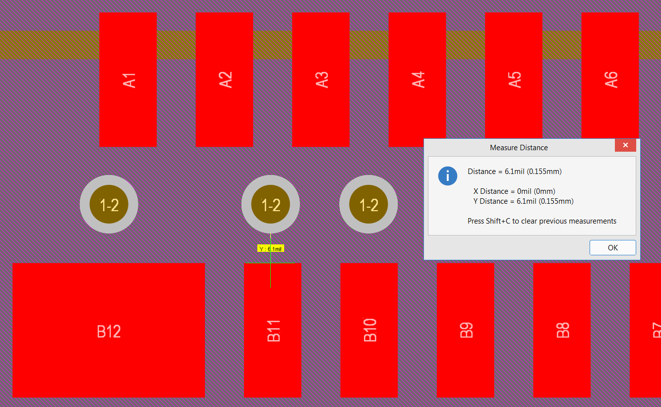
I just put the footprint into Altium to get a better sense of the size. I am able to fit a via with an 8 mil drill (0.203mm) and a 12 mil pad (0.305mm) between the rows of pads. These are not unusual sizes for vias either, and will not cost you extra (unless you're looking for 10 mil clearance (0.254mm). Using this size via provides more than 5 mil of clearance on either side (minimum of 0.132mm).

enter image description here

\$\endgroup\$
5
  • 1
    \$\begingroup\$ Just as a note, it certainly could cost you extra. My own supplier does charge more for that via geometry. It's always a good idea to check, if just to avoid unpleasant discoveries when it does go to fab. \$\endgroup\$
    – Cursorkeys
    Commented Jun 11, 2019 at 11:55
  • \$\begingroup\$ The copper definitely fits - but you haven't shown the solder mask expansion. If you add a solder mask expansion of even 2mil, the solder mask sliver becomes tiny, like 1-2 mils thin... what to do about that? \$\endgroup\$
    – VanGo
    Commented Jun 11, 2019 at 16:32
  • \$\begingroup\$ @Cursorkeys Fair point, definitely check with the supplier first. Most regular board houses won't charge extra until you go less than a 6 mil drill, at which point it is considered micro-vias \$\endgroup\$
    – DerStrom8
    Commented Jun 11, 2019 at 22:49
  • 2
    \$\begingroup\$ @VanGo simply tent the vias. Don't add soldermask expansion \$\endgroup\$
    – DerStrom8
    Commented Jun 11, 2019 at 22:49
  • \$\begingroup\$ @DerStrom8 that seems like the best idea - thanks for the suggestion! \$\endgroup\$
    – VanGo
    Commented Jun 12, 2019 at 1:27

Your Answer

By clicking “Post Your Answer”, you agree to our terms of service and acknowledge you have read our privacy policy.

Not the answer you're looking for? Browse other questions tagged or ask your own question.