1
\$\begingroup\$

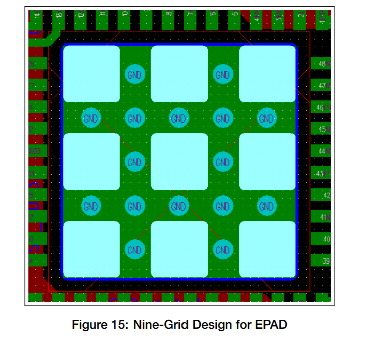
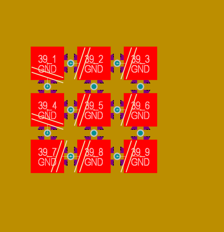
I have a component with a land pattern I haven't routed before. Usually thermal pads have the vias in them so the connectivity is obvious. However, in this case the vias are placed between the pads. My understanding is this is a way to stop the solder from sinking into the vias.

I'm routing a 4 layer board so I'm wondering what the best way to connect this is. Is the intention here to just connect all the pads to the vias?

The second image is from the datasheet which contains the land pattern.

enter image description here

enter image description here

\$\endgroup\$
5
  • \$\begingroup\$ Are you sure the footprint is correct? That looks suspiciously like the design has confused the solder paste stencil diagram with the pad layout. \$\endgroup\$ Commented Mar 14, 2021 at 18:32
  • \$\begingroup\$ Pretty sure @TomCarpenter -- from the data sheet this is the suggested land pattern (updated question to display) \$\endgroup\$
    – jsinglet
    Commented Mar 14, 2021 at 22:54
  • \$\begingroup\$ Is the component secret? \$\endgroup\$
    – pipe
    Commented Mar 14, 2021 at 23:04
  • \$\begingroup\$ Yeah, so that's showing one large ground pad, with one single solder mask openning, but with 9 smaller areas of solder paste. \$\endgroup\$ Commented Mar 14, 2021 at 23:04
  • \$\begingroup\$ @TomCarpenter -- this is the component: espressif.com/sites/default/files/documentation/… \$\endgroup\$
    – jsinglet
    Commented Mar 15, 2021 at 0:51

1 Answer 1

1
\$\begingroup\$

Updated Answer - Based on Link In Comments

Right, so The image you posted of a nine-grid EPAD and the link you posted in the comments are completely different. One is a QFN package, and the other is a PCB module.

In the case of the linked part, there are 9 seperate pads, because the module itself has 9 seperate solder pads underneath it, rather than one large one. (though apparently looking at images, some variants have one pad, others have 9)

Assuming the dimensions are correct, the pattern you show in your first image appears to match.

There is nothing in the datasheet that prohibits having ground underneath the module, so you could easily connect everything with a ground plane on the top layer.

Furthermore, you don't actually need to solder the pad accorting to the datasheet, its connection is optional. If you are to connect it, they recommend ensuring that the amount of solder paste is minimised, which is why they have nine small pads for the paste layer.

The vias are there not to allow paste to wick away. They are intended to provide thermal transfer - copper is a better conductor than FR4, so having the vias allows the heat to escape onto inner copper layers and the reverse of the board.


Previous Answer - Based on the Figure 15 Image

Looking at the figure you've posted, I think the footprint you are using has perhaps confused the actual land pad for the solder paste.

"Figure 15" shows a QFN package with a single large central pad (green) with a single solder resist openning (blue).

The solder paste stencil is then to have 9 opennings (light blue) rather than one large openning. This is done to reduce the amount of solder under the device, which becomes necessary on larger QFNs. A 100% fill density could cause the device to float on the solder and prevent the pins from properly connecting.

\$\endgroup\$
1
  • \$\begingroup\$ In other components this sort of thing is handled by putting vias in the pads directly. However the solder leaks. Isn't it reasonable to just put those vias in the grid described and route the ground pads to the vias? According to the data sheet the large squares are supposed to be connected to GND. \$\endgroup\$
    – jsinglet
    Commented Mar 15, 2021 at 0:55

Your Answer

By clicking “Post Your Answer”, you agree to our terms of service and acknowledge you have read our privacy policy.

Not the answer you're looking for? Browse other questions tagged or ask your own question.