2
\$\begingroup\$

I see in the guides to standard Bipolar Transistor circuits (emitter-follower, common emitter amplifier), they always say: Choose a quiescent current of 1mA.

How is this value chosen? I look at the specification sheets and I am not sure what I am looking for specifically. From my understanding it should be based on the output characteristics of the transistor so that clipping does not occur and maximum symmetrical swing is obtained. However, I have to use the 2N3904 transistor, and the spec sheets don't have the output characteristics. I also have to drive a load of 100k ohms. Does choosing a quiescent current depend on the load?

\$\endgroup\$
12
  • \$\begingroup\$ One thing I would definitely not do first when designing a transistor amplifier is: Choose a quiescent current of 1mA. That's my cunning plan and don't assume I'm Baldrick LOL. \$\endgroup\$
    – Andy aka
    Commented Oct 16, 2019 at 11:46
  • 1
    \$\begingroup\$ That 1mA is just an example / starting point. The most optimum biasing current depends on the transistor and what you want to do with it. For example, high frequency transistors often have a biasing current value that will result in the highest bandwidth. Another example: for an Audio stage driving a speaker of 8 ohms, a 1 mA biasing current is extremely low considering that more than 1 A can flow in normal operation. \$\endgroup\$ Commented Oct 16, 2019 at 11:49
  • \$\begingroup\$ let Ic*Rc = V+/2 then let Ib = Ic/ hFE (100 ish). Vb will be <600 mV with a current limiting Bias from Vref with R divider Ohm’Law then AC couple In faster than input swing V/ T(=RC ) slew rate. Add Re and choose gain = Rc/Re \$\endgroup\$
    – D.A.S.
    Commented Oct 16, 2019 at 12:03
  • \$\begingroup\$ If you are stuck using a specific BJT (because that's already been decided for you), then you can find the range of collector currents over which it is useful (typically, this is two to three orders of magnitude range -- so you have many options, still.) It's possible you have a specific battery system (button battery or 9 V battery) and this may, taking into account the entire circuit functions, also suggest some limiting boundaries. (A teacher could demand the value.) But if you were to write down a list of specs, I think others may help you re-orient yourself with respect to this question. \$\endgroup\$
    – jonk
    Commented Oct 16, 2019 at 20:01
  • \$\begingroup\$ @Andyaka I also, wouldn't firstly choose Icq. But these are steps we have to follow, so I just trying to figure out the justification behind this assumption. \$\endgroup\$ Commented Oct 22, 2019 at 2:22

3 Answers 3

1
\$\begingroup\$

Some considerations that constrain the range of values you would choose for an application:

  1. Battery operated devices will need to draw as little current as possible from the battery, to prolong battery life. A 1Ah battery will be able to source 10mA for 100 hours, so if you design a circuit with 10 elements each requiring 1mA, is 100 hours enough?

  2. Things get hot as they dissipate power. 1mA through 1kΩ dissipates \$ P = I^2 \times R = 1mW\$, barely noticeable to the touch. 10mA through 1kΩ is 100mW, quite warm. Clearly, if you can use less current, then do so. Heat management is a huge part of many designs.

  3. Resistors are noise sources and antennae. Much of design work is to mitigate pickup from the surroundings, and noise generated, and in this context lower resistor values are better. Chosen values will be a compromise between immunity to noise and pickup, and power consumption. Some transistors are designed for low-noise performance, and collector current will be chosen to operate them where they are least noisy.

  4. For most signal designs the voltages used are of the order of 10V. Designs working at 100V or 1V are hard. That immediately places constraints on the range of circuit conditions you have available to you.

The "jellybean" value of 1mA you ask about is really just a compromise that satisfies those considerations. Given voltages of the order of 10V, a current of 1mA implies the use of resistances in the kilohms, not ohms or megohms, which also happens to have reasonable noise and pickup immunity in most applications.

The value 1mA itself tells you something about why it was chosen. It's not 0.75mA or 1.2mA, it's just 1 something. it is really intended to imply an order of magnitude, and you have flexibilty to manoeuvre around that. It may perfectly OK to jump up or down one order (or more) between 100μA and 10mA, for example. Everything depends on the application and the constraints imposed on it from other directions.

Your own application needs to drive 100kΩ, and (assuming you are not concerned with power transfer), your main concern is probably obtaining an output impedance significantly lower than that, to avoid distortion. Therefore a collector resistor of 100kΩ is not going to cut it. That would imply a collector current on the order of \$ I = \frac{10V}{100k\Omega} = 100\mu A\$. A smaller resistor is required, say 1kΩ, for a collector current of order \$\frac{10V}{1k\Omega} = 10mA\$.

It seems that a suitable resistor value would be somewhere in between those two extremes, and the resulting collector current would be somewhere between 100μA and 10mA. So, even in your own example application, 1mA is a good starting point!

\$\endgroup\$
1
  • 1
    \$\begingroup\$ In today's design space, I actually consider 1 mA to be pretty much on the high end. I have used designs with 1 uA quiescent current, but rarely more than 1 mA \$\endgroup\$
    – tobalt
    Commented Jun 11, 2022 at 5:45
0
\$\begingroup\$

This circuit will give you 1MHz bandwidth, and drive a 100Kohm load with less than 10% error because of the load resistor.

Your gain (notice I made this YOUR circuit) will be 10K||13K / (1K + 26 ohms) where the 26 ohms is the small_signal gradient of the diode equation for certain diode dopings, also useful for transistor transconductance thinking.
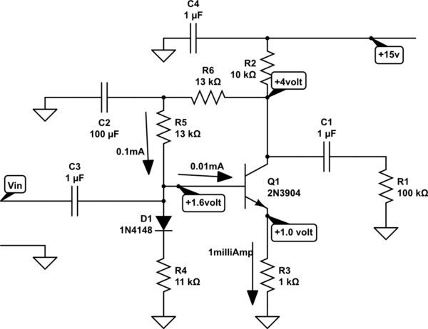
schematic

simulate this circuit – Schematic created using CircuitLab

What dos this schematic illustrate?

--- the 100K load resistor is 10x the Collector resistor, thus there is less than 1 dB gain error (1dB = 12% voltage ratio)

--- the bandwidth (at the collector), with NO ALLOWANCE for any Cload across the 100Kohm, is approx. 10Kohm in parallel with 10picoFarad, the Cob of 2N3904 (from my memory). In truth we should include the DC_biasing feedback resistor of 13K to be in parallel with the 10K. Ignoring that for now, as we approximate the collector TAU to arrive at the bandwidth, we have 10K ohm * 10pF = 100 nanosecond. Since this is a 1-pole approximation, just invert that and divide by 6.28 to have bandwidth being 1.59MHz.

--- the gain is roughly Rcollector/Remitter (10Kohm/1Kohm); for more accuracy, read the 2nd paragraph of this answer

--- input resistance? so you might compute loading effects on any sensor or voltage source such as a prior stage? R4 || R5 || (Beta * R3)

--- input impedance? Cmiller will make the Cin be (1 + Av) * 10pF; you can cascode this circuit, and reduce that to (1 + 1) * 10pF

--- distortion? if I recall rightly, 4 milliVolts across the emitter-base will produce 10% distortion of collector current; however there is a linearization resistor in the emitter, of value 1,000 ohms. The ratio of 1,000 / 26 is the distortion-improvement ratio, which is 39:1. Thus the distortion for 4 milliVolts input (across EB and Remitter) will be 10% / 39 or 0.25%.

Again this is for 4 milliVolts input. For fun, set up a SPICE simulation, alter the Vin to be 4mVPP, include .fourier behavior, and examine the result.

\$\endgroup\$
2
  • \$\begingroup\$ Thanks for the feedback but I not really looking for a solution, I am trying to understand why a value of 1mA is chosen. Does this come from the datasheet and if so, what specifically am I looking at to find this value. What if I choose something like 10 mA, how would that affect the result. \$\endgroup\$ Commented Oct 22, 2019 at 2:20
  • \$\begingroup\$ given your load of 100,000 ohms, at 1mA the voltage would be 100 volts. Since that is a very large voltage, we can assume only a small portion of the collector current will go thru the Rload, and the rest will continue thru the collector resistor. This, most of the current remaining in the collector resistor, is important for low or moderate distortion, and I assume that is also one of your goals. \$\endgroup\$ Commented Oct 25, 2019 at 10:48
0
\$\begingroup\$

1mA is just a typical and convenient value for the collector current.

The higher the chosen collector current, the lower can be the value of the collector resistor to achieve mid-supply dc biasing. Since the collector resistor nominally defines the output resistance of a common emitter amplifier it means that a lower value collector resistor results in less reduction in the amplifiers gain due to the potential divider formed between the collector resistor (output resistance) and the load resistance which is often the input resistance of the following stage.

The drawback of a higher chosen collector current is that more power is dissipated in the amplifier and so choosing the collector current is a trade off between gain and power dissipated (power drawn from supply).

\$\endgroup\$
1
  • \$\begingroup\$ 1mA is a convenient value for a small signal amplifier. Now imagine the collector current in a common emitter power amplifier. 1mA isn't going to cut it for a 1 watt output amplifier unless you use an awful high voltage power supply. \$\endgroup\$
    – JRE
    Commented May 7, 2021 at 15:39

Your Answer

By clicking “Post Your Answer”, you agree to our terms of service and acknowledge you have read our privacy policy.

Not the answer you're looking for? Browse other questions tagged or ask your own question.