There are quite a number of things that will do this to you.
You have not stated the length of the interface. I do direct chip to chip PCIe frequently and you really need to take this into account as you will get attenuation of roughly 0.18dB per inch due to skin effect losses and about 0.5dB per inch due to dielectric absorption on 'ordinary' FR4.
I think you may be able to get better numbers from the PCB material datasheet if you download it and look at the loss tangent. Take a look at Isola 370HR for a typical datasheet. The numbers above are pretty accurate at the 5GHz rate. At the 2.5Gb rate, the numbers are a bit lower, with a total loss of ~ 0.4dB per inch.
I am assuming that apart from breakout and the coupling capacitors, you are using single-layer routing for the interface. Layer transitions can easily do very nasty things to the signal. Controlled impedance will be a bit different layer to layer and reflections are the natural result (there are ways of successfully doing multi-layer routing, but it takes a great deal of care and some unusual tricks to achieve).
For PCI express (and Infiniband for that matter), the rise and fall rate of the signal at the transmitter has a minimum rise and fall time to minimise EMI issues, and that time is 0.25UI, which yields 10GHz signalling artefacts on gen 2 links and 5GHz artefacts in gen 1 which must be taken into consideration.
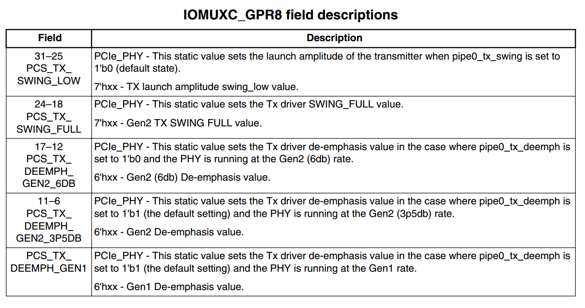
The de-emphasis field above helps you get a clean eye at the receiver by bringing the non-switching amplitude down relative to the nominal launch amplitude.
If you are losing too much amplitude at the switching edge of the signal, set this field to a larger value. You might also set the nominal launch amplitude a bit higher as well.
Other issues you may look at:
Where, relative to the transmitter, are the coupling capacitors? They should be as close to the transmit pins as possible. Once they are more than half a wavelength of 10GHz (about 0.6 inches on FR4) [double that distance for 2.5Gb/sec links], they will most definitely reflect energy.
I have had problems with capacitor geometries of 0402 or larger in PCI express gen. 2 and I now use reverse geometry devices (0204) for the reduced effective series inductance. These seem to be getting the job done very well.
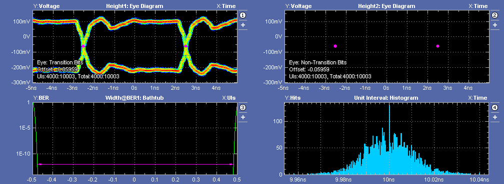
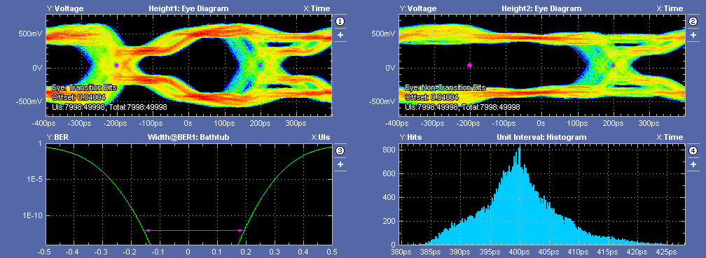
Looking closely at the eye diagram for transition bits (nice scope you have, by the way - that is what you need for this stuff), the initial signal drive appears to be driving a terminated line (the signal goes to 0.5 V(nominal) in the classic transmission line manner). This is not a particularly long line (the round trip time is where the signal drives to full V[nominal]).
you say that the link is running at 2.5Gb/sec (gen 1) and that is what the scope traces show, but you may want to experiment with the de-emphasis field (look in the reference manual as well as the electrical data sheet (see note below). The 'standard' de-emphasis values are for a nominal link, not an embedded link such as you have here (and what I also do regularly). If you can get it to about 6dB, you may get better results.
The nominal de-emphasis is 3.5dB for Gen 1 and 6dB for Gen2. I note that the field above seems to imply that a Gen 2 link is 3.5dB - you may want to dig a bit on that. The link you have needs a minimum of 3.5dB of de-emphasis.
Note that the eye at the receiver will be very different, but this is where it matters. As an experiment, read the error counters in the processor (most of them have a counter for retries); if you are not seeing significant errors, you may be chasing something that is not really a problem. If you are seeing large error counts, then maybe some of this might help.
One more thing: excessive launch amplitudes and de-emphasis are just as bad as setting them too low.
Maybe that will help you a bit: Hope so.
Note: Freescale documents everything, it is just that sometimes it is not in the place you expect to find it. Make sure you have the latest device errata as well.
Update. Added notes about capacitor geometries.
Up to the 2.5Gb/sec node, 0402 devices are fine. My handy calculator shows a typical 0402 device has about 10 ohms of impedance (inductive) at this frequency and 21 ohms at 5GHz (the highest frequency of interest). This is not too bad in a 100 ohm differential system as the effective impedance of a closely coupled pair is somewhat less than a straight addition.
The self resonance for this device is 19MHz, well below all frequencies of interest, so any phase noise is due to ESL. Keeping the impedance down to less than about 1/3 of the effective track impedance means that the phase noise (and therefore additional ISI) we will get is between 1 and 17 degrees (a single ended track from a closely coupled pair is typically (Z(diff)/2)*1.25, so for 100 diff, the single ended impedance is about 65 ohm). This amount of phase noise is manageable.
At 10GHz, the effective impedance is about 44 ohms, and can start to interfere with the differential pair by introducing excessive phase noise across the frequency band of interest as the maximum phase is now about 34 degrees. Although I have successfully done Gen 2 with 0402 devices, I have also had issues with longer runs and now use 0204 reverse geometry devices for this speed and higher.
For 8b/10b encoded links, the frequency band of interest is from bit rate/5 to bit rate * 2. The lower limit is bounded by run length encoding, and the upper limit is bounded by the specification requirement for minimum rise and fall times.
The ESL for various geometries:
0402: about 700pH
0204: about 300pH
0805: about 1nF
Update Added commentary about 50% initial launch amplitudes.
Let us consider a transmission line terminated at the source and destination at the characteristic impedance of the line, Z0.
At the initial launch, assuming the line is long compared to the wavelength of the signal, the launching point will go to 50% of launch amplitude due to voltage divider effect (the transmitter sees only the transmission line at this point).
Once the energy arrives at the destination point and starts rising to the 50% point, the energy at the source has effectively 'filled' the line with energy and rises to the full launch amplitude. Strictly speaking, the transmission line at the destination sees a voltage divider, and the divider effect at the source disappears as the output approaches DC (keeping in mind that the transmission line effect is applicable only to transitions).
This could also be visualised as the 50% energy level moving down the transmission line to the final termination and then reflecting back at full level. That is why we see a 'round trip time' in the 50% point at any point on the line.
Your plot shows precisely this behaviour at a point in the line that is not yet at the destination port, because this 50% point is in fact moving along the line.
At the receiver, once the energy has reached to 50% point, the full energy of the line is following and the voltage at the receiver continues to rise, giving a smooth transition from one level to the other.
This could also be visualised as the 50% voltage point moving along the line to the receiver, then reflecting back at 100% (the receiver achieves DC first). For that reason, the voltage at 50% viewed at any point on the line shows the round trip time from that point to the receiver.
This discussion is as valid for differential signals as single ended.
So your plot above shows classic transmission line behaviour with little excursions beyond the expected behaviour. In fact, this is one of the cleanest transmitter eyes I have seen.


