0
\$\begingroup\$

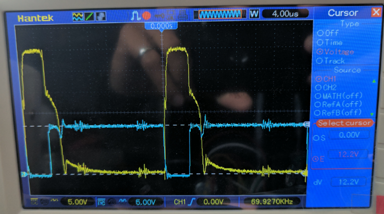
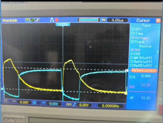
Below is the picture of my gate drive signals. The blue trace is the low side gate signal and the yellow trace is the high side gate signal. Both signals are measured across the gate and source of the high and low side mosfets.

enter image description here

As you can see the high-side gate signal (yellow trace) is falling very slowly. Why is this the case? I am using an NCP5181 as my gate driver.

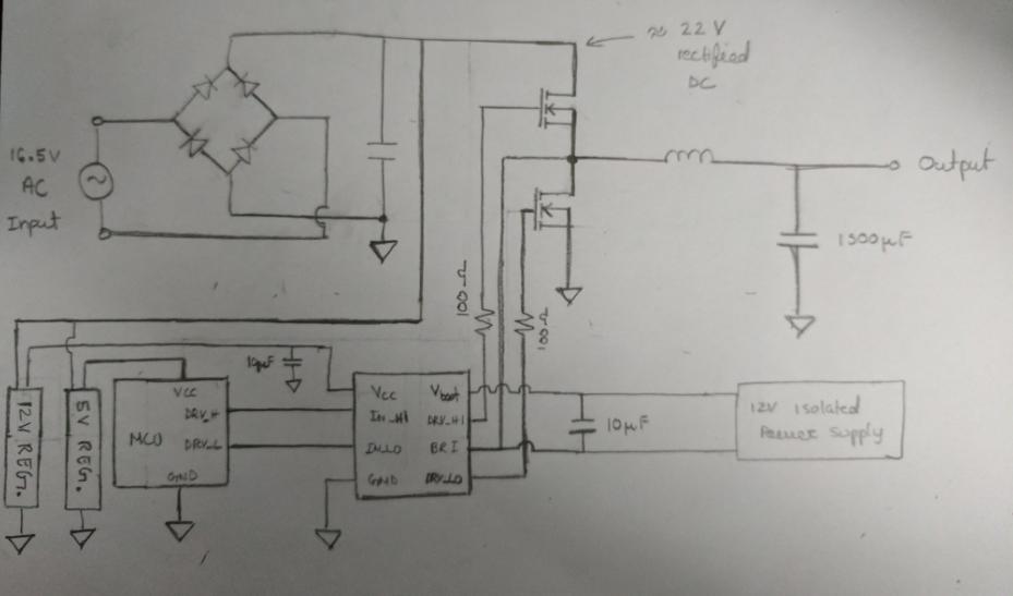
Below is my circuit.

enter image description here

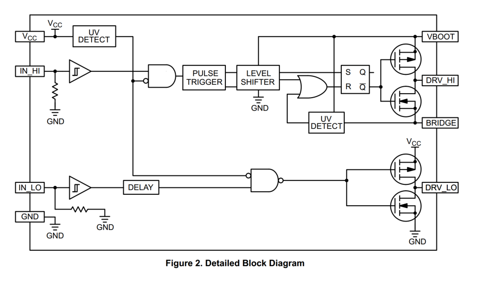
For completeness, below is the block diagram of my gate driver IC. In the block diagram of the datasheet it shows that the high side is driven low by a push-pull MOSFET configuration so I would think that the gate signal should go low quickly.

enter image description here

For reference here are the scope signals when they are both measured with reference to the ground of the circuit.

enter image description here

\$\endgroup\$
13
  • \$\begingroup\$ How are you probing both outputs? The blue trace looks like it's swinging to -5vdc when the high side driver switches \$\endgroup\$
    – sstobbe
    Commented Jun 2, 2017 at 21:35
  • 2
    \$\begingroup\$ Show your exact circuit. \$\endgroup\$
    – Andy aka
    Commented Jun 2, 2017 at 21:46
  • 1
    \$\begingroup\$ As Andy aka says, show your circuit. Most particularly show your load. If the DRV_HI output is floating, then a high output will drive quickly to Vcc, but a low output will simply discharge the output capacitance very slowly. \$\endgroup\$ Commented Jun 2, 2017 at 23:01
  • \$\begingroup\$ @OlinLathrop I think you're confusing the block diagram of the driver IC he's using with his circuit schematic (which is not included/shown). \$\endgroup\$
    – W5VO
    Commented Jun 2, 2017 at 23:26
  • 1
    \$\begingroup\$ With 100Ω gate resistors, you're not going to see that fast of a gate transition, but I suspect that isn't the reason you're having issues. You haven't mentioned which power MOSFET you're using. That oscilloscope can't do two isolated differential measurements without additional equipment - this is a common beginner's mistake which is why exact connection points for each probe are necessary for further information. \$\endgroup\$
    – W5VO
    Commented Jun 3, 2017 at 3:51

2 Answers 2

3
\$\begingroup\$

Comment from the OP: -

The probes are connected between the gate and source of both MOSFETs directly.

Here's where you are likely screwing up. The ground connection on the probes are connected to each other to local ground on the oscilloscope so, in-effect, you are shorting out the lower MOSFET from drain to source.

If you want to do this properly use two probes that have their ground connection to 0V on the target circuit and probe the gate and the source of the top MOSFET. Look at the differential voltage by using the appropriate function on the o-scope.

Make sure both o-scope channels are set to DC.

\$\endgroup\$
3
  • \$\begingroup\$ I think Andy has identified your largest issue with probing, but also watch out for the isolation bench-top power supplies, while they provide good DC isolation, the transformer winding form a big capacitor to mains ground. I would use a 9V or 12V battery for your isolated supply before eventually going to a bootstrapped supply. \$\endgroup\$
    – sstobbe
    Commented Jun 3, 2017 at 13:22
  • \$\begingroup\$ Thanks for the info, I will keep in mind the reference of my scope connections. Also, I have posted the measurement with both gate signals measured with reference to ground, it still seems that there is a delay that happens in the fall time of the high side drive. \$\endgroup\$ Commented Jun 4, 2017 at 0:43
  • \$\begingroup\$ Should have figured thats basically a short....I will try to do the differential voltage measurement aswell. \$\endgroup\$ Commented Jun 4, 2017 at 0:50
-2
\$\begingroup\$

This usually happens when designers fail to recognize the impedance ratios of RdsOn of the gate driver and RdsOn of the power switch.

But in your case with updated info your gate resistor is too high and Boost cap may be too low or commutation rate.

Replace 100 ohms with 5 Ohms to closer to matched driver impedance as long as the Boost cap is not decaying too fast.

It is a known characteristic that the gate charge Q and Ciss is inversely proportional to RdsOn. This also applies to Coss. So when commutation occurs you have a nonlinear C near Vth threshold of Vgs that rises sharply when turning on after some latency period.

The other known characteristic is some bridge drivers tend to have higher Rdson for Pch/Nch ratios. In this case ratio=2.5x nominal and lower worst case at max RdsOn. However since your question and design is incomplete, the ratios of Ciss for your output stage need to be factored with the model of driver impedance. I won't draw the model, but it is like a switched capacitance at threshold of switched resistance. So one would expect using this chip that the high side will be slower turn ON and turn OFF than the low side.

Great care must be taken in choosing your power drivers for many parameters affect RdsOn, Ciss and Coss such that the figures of merit FoM are the time constants RC=T for different stages, off, transition and On.

I prefer to start by ensuring the Power Switch RdsOn is not less than 1% of the prior stage RdsOn for fast gate transition times. But in high power devices this must be drive/output switch resistance ratio may need to be increased to 10%, which is why IGBT's are more popular having exceptionally low output RC= Times for the BJT output and with equally low input. T= Ciss *Rg thus fast slew rates for the low current MOSFET inputs.

Review your design in light of these parameters and please improve the details in your overall design with full schematic, layout and loads.
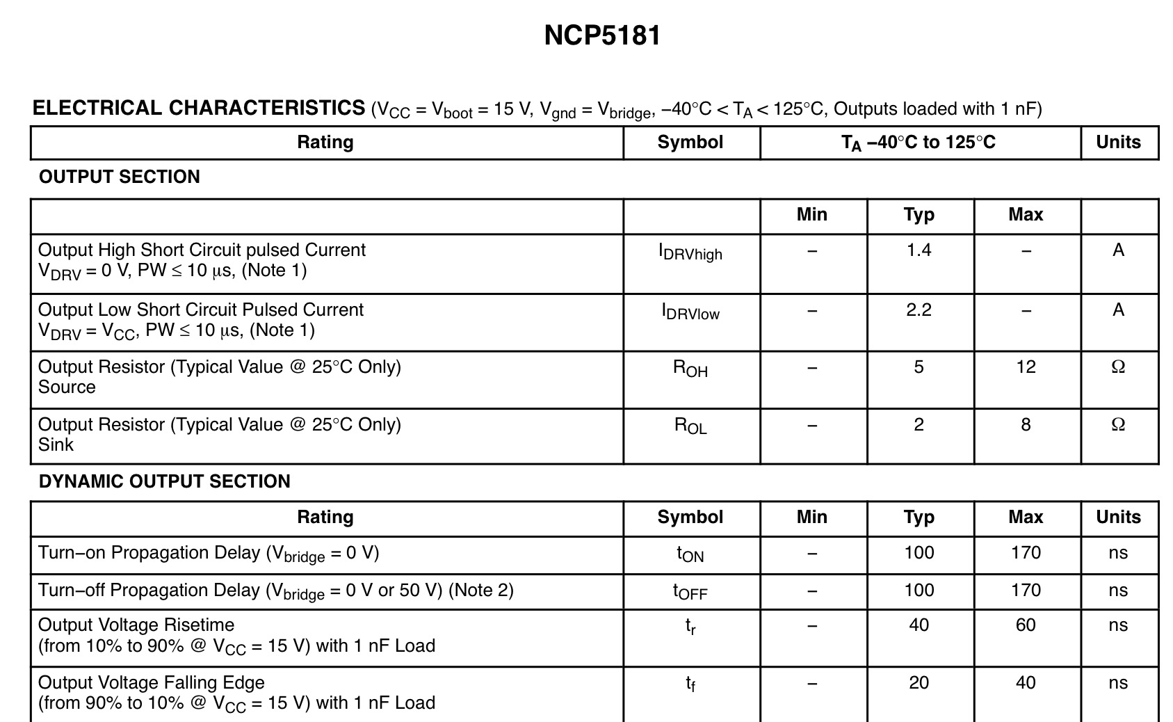
enter image description here

Finally where the output drive not shown is wired OR, you must ensure the results of Gate driven T slew rates do not reduce the dead-time needed to prevent shoot-thru and thus are momentary break before make on the order of 1us +/- 50% or more depending on RdsOn/L load.

\$\endgroup\$
5
  • \$\begingroup\$ Thanks for the comprehensive answer! Just to make sure I understand correctly the main take away is to look at the Rdson of my gate driver (NCP5181) and to ensure it is low or to consider using IGBTs because of their faster switching capability. Also what does "I prefer to start by ensuring the Power Switch RdsOn is not less than 1% of the prior stage RdsOn for fast gate transition times" mean? Would the prior stage in my circuit be the rectifier? Appreciate your help. \$\endgroup\$ Commented Jun 3, 2017 at 3:18
  • \$\begingroup\$ your output switches are undefined and possibly you make need a lower Ciss value was my main point. or... else the NCP5181 is not low enough RdsOn the driver them... or maybe you need intermediate drivers like to go from 5 to 0.1 to 0.02 using 50:1 ratio .. in any case there are many solutions and thousands of choices. Your choice obviously isnt working. The main problem is your lack of,specs and lack of details supplied. \$\endgroup\$
    – D.A.S.
    Commented Jun 3, 2017 at 4:12
  • \$\begingroup\$ I just saw your 100 ohm R's . no wonder your RC time constant is so slow .. match the series R and Rdson to the output are value, also. How ground shift can you measure? \$\endgroup\$
    – D.A.S.
    Commented Jun 3, 2017 at 4:28
  • \$\begingroup\$ In terms of the ground shift, how do I know if this is happening? \$\endgroup\$ Commented Jun 4, 2017 at 0:44
  • \$\begingroup\$ locate ground probe near source measure output ground and beware of radiated noise from probe ground. Although better method is 50 ohm terminated coax. to different grounds keeping center wire shielded to see on scope. Did you try replacing 100 ohms with 5 Ohms yet? \$\endgroup\$
    – D.A.S.
    Commented Jun 4, 2017 at 1:08

Your Answer

By clicking “Post Your Answer”, you agree to our terms of service and acknowledge you have read our privacy policy.

Not the answer you're looking for? Browse other questions tagged or ask your own question.