0
\$\begingroup\$

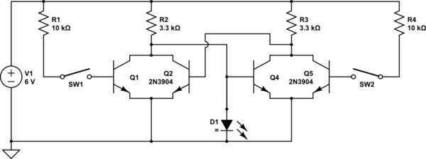
I am trying to create an SR Latch with two NOR logic gates that lights an LED. I am implementing the gates using 2 transistors and 2 resistors each.

Here is the schematic:
schematic

simulate this circuit – Schematic created using CircuitLab

The goal is for Switch 1 to be the Reset button and for Switch 2 to be the Set button. My concern is if there will be enough current to light up the LED (I am hoping to get 5mA-20mA flowing through it).

I am confused on how to find the resistance and current because different paths split into multiple other parallel paths. (i. e. the path that \$R_2\$ is on splits into two, and one of those paths splits into two more)

I know that \$\frac{1}{R} = \frac{1}{R_1} + \frac{1}{R_2} + ...\$ and that \$I = V(\frac{1}{R_1} + \frac{1}{R_2} + ...)\$ But how do I apply this to the different paths of the circuit?

I would like to know how to find how much current is flowing through a component and how much resistance is on a path in schematics similar to this one (meaning they use logic gates implemented similarly).

\$\endgroup\$
1
  • 3
    \$\begingroup\$ The forward biased base-emitter voltage of an NPN silicon transistor will be about 0.7 volts (same as a silicon diode), so the LED can never light - it would require about 2 volts, depending on colour. \$\endgroup\$ Commented Dec 10, 2017 at 22:50

2 Answers 2

0
\$\begingroup\$

Move the LED. Add a current-limiting resistor in series with the LED, and place that series R_LED combo in parallel with R2. Try 100 ohms in series with LED.

\$\endgroup\$
0
\$\begingroup\$

Trying to reinvent the SR latch wheel?

There are a few problems not worth solving with your design.

  • Vbe4 < Vf of D1 so D1 never turns on. Even if resolved that there is no reason to use so many discrete parts when 2 NAND or 2 NOR gates will work as an SR latch.

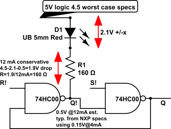
in any case assuming LED was on If= (5V-Vf)/3.3k


schematic

simulate this circuit – Schematic created using CircuitLab

If using standard 74HCxxx logic, I might derate 20mA LED to 12 mA and calculate R for 12 mA using datasheet for 74HC00 NAND with Vol at 4.5V for V+.

This is the classic SR latch using 2 NAND gates with active logic low inputs. (!)

\$\endgroup\$
3
  • \$\begingroup\$ Thanks for your answer. I just wanted to make it for learning purposes. I guess I just don't understand how to find Vbe4. \$\endgroup\$
    – alexm
    Commented Dec 10, 2017 at 21:58
  • \$\begingroup\$ Vbe4 is about 0.7V when biased on and 0.2V when off from Q1 or Q2 s o the LED Vf of ~2V for R/Y or ~3V for G/B/W would never work. \$\endgroup\$
    – D.A.S.
    Commented Dec 11, 2017 at 2:51
  • \$\begingroup\$ You can examine 1970 datasheets for discrete TTL NOR gates to look at datasheets or web images for SR FF , here dual gate SR latch and 2 more gates turns into JK FF electronics-tutorials.ws/sequential/seq13.gif It is better to learn how it was done than guess. \$\endgroup\$
    – D.A.S.
    Commented Dec 11, 2017 at 2:53

Your Answer

By clicking “Post Your Answer”, you agree to our terms of service and acknowledge you have read our privacy policy.

Not the answer you're looking for? Browse other questions tagged or ask your own question.