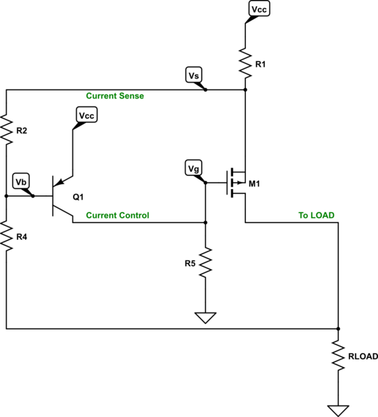
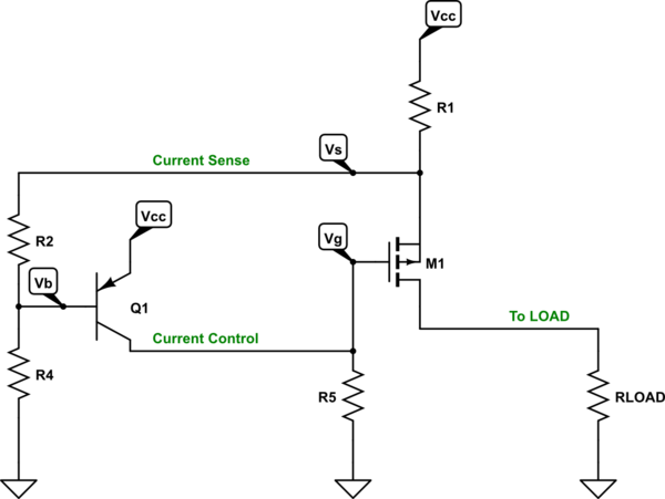
Redrawn, the circuit looks like this:

simulate this circuit – Schematic created using CircuitLab
Just a small re-arrangement that may make things just a little easier to see.
The basic idea is that \$M_1\$ passes \$V_\text{CC}\$ along and over to the load, but that \$R_1\$ is inserted so that \$V_s\$ can provide a changing voltage that varies based on the load's behavior.
To start out, the circuit does the easiest thing to make something happen, which is to simply turn \$M_1\$ on. That's \$R_5\$. Without anything else attached to \$R_5\$, there will be no gate current in \$M_1\$ and so \$R_5\$ won't drop any voltage and so the gate will just be grounded and therefore uncontrolled. So the load would see pretty much \$V_\text{CC}\$, except for a small drop across \$R_1\$ and across \$M_1\$.
Of course, something needs to control \$M_1\$. What's really nifty here is that with \$R_5\$ present, all one has to do is sink current into it and it will drop a voltage. That will jack up \$M_1\$'s gate. If enough current sinks into \$R_5\$, and given the way \$Q_1\$'s emitter is wired directly to \$V_\text{CC}\$, the gate could even be driven very close to \$V_\text{CC}\$ if \$Q_1\$ is driven into saturation. (But you don't need to consider that, because long before \$Q_1\$ goes into saturation there will not be enough difference between \$V_g\$ and \$V_s\$ and \$M_1\$ will be off. So expect that \$Q_1\$ will stay in its active mode.)
This means that \$Q_1\$ has the job of monitoring the current sense line and sourcing current that \$R_5\$ will sink, as needed. In active mode, \$Q_1\$'s collector acts like a current source. (Changing over to a voltage source when \$Q_1\$ is saturated.) Such an arrangement is a really good match for sinking current into \$R_5\$.
The current sense line draws a small amount of current. For the purposes of a simple analysis, the simpler presumption is that it draws no current at all. (A designer would make sure that the current sense requires far less current than the load.) So this allows us to see \$R_2\$ and \$R_4\$ as a simple voltage divider. (We should also assume that \$Q_1\$'s base doesn't require any current, to keep things simpler.)
So it must be the case that \$V_s=V_\text{CC}-I_\text{LOAD}\cdot R_1\$. And therefore, \$V_b=\frac{R_4}{R_2+R_4}\cdot V_s\$. This then means that the base-emitter junction voltage magnitude for \$Q_1\$ will be \$V_\text{CC}-V_b\$.
Remember the rule that a \$60\:\text{mV}\$ change in \$V_\text{BE}\$ means a 10X change in collector current!! So it doesn't take much change of \$V_b\$ to make a huge change in the collector current and therefore a big change in the voltage drop across \$R_5\$. Because of this fact, we can assume that there is some \$V_\text{BE}\$ for \$Q_1\$ before which there is not much voltage drop across \$R_5\$ and after which there is enough to shut off \$M_1\$. It happens fast, that way.
The only question we might have is about what magnitude of \$V_\text{BE}\$ is this transition. To look at that, we simply look at \$\frac{V_\text{CC}}{R_5}\approx 150\:\mu\text{A}\$. With that much collector current (and it is not much), \$M_1\$ will be all the way off. So we know the collector current will be still less. This means that \$V_\text{BE}\$ will be perhaps near \$620\:\text{mV}\$ by the time the transition is complete and \$M_1\$ is off. Still less than that, or perhaps around \$620\:\text{mV}-60\:\text{mV}=560\:\text{mV}\$, when the transition starts. This means we can just "pick a number" that is somewhere between these two values and know that it will be about right.
The overall equation is then:
$$\begin{align*}
V_\text{BE} &= V_\text{CC}-V_b\\\\
&= V_\text{CC}-\frac{R_4}{R_2+R_4}\cdot V_s\\\\
&= V_\text{CC}-\frac{R_4}{R_2+R_4}\cdot \left(V_\text{CC}-I_\text{LOAD}\cdot R_1\right)\\\\
V_\text{CC}-V_\text{BE} &=\frac{R_4}{R_2+R_4}\cdot \left(V_\text{CC}-I_\text{LOAD}\cdot R_1\right)\\\\
I_\text{LOAD}\cdot R_1 &=V_\text{CC}-\left(V_\text{CC}-V_\text{BE}\right)\frac{R_2+R_4}{R_4}\\\\
I_\text{LOAD}&=\frac{V_\text{BE}\left(R_2+R_4\right)-V_\text{CC}\:R_2}{R_1\:R_4}
\end{align*}$$
Another way to look at the above is to set \$\alpha=1+\frac{R_2}{R_4}\$ and then to compute:
$$I_\text{LOAD}=\frac{\alpha\:V_\text{BE}+\left(1-\alpha\right)V_\text{CC}}{R_1}$$
The factor, \$\alpha=1+\frac{R_2}{R_4}\$, makes the resistor divider the star of the show, so to speak. And also highlights \$R_1\$'s current-limit role instead of conflating it with \$R_4\$.
For the value of \$V_\text{BE}\$, you should use some value between the limits I mentioned earlier. Probably something near \$600\:\text{mV}\$, given the values in your schematic.
If you know the load current limit you want, this tells you that the resistor divider, \$R_2\$ and \$R_4\$ must use perhaps 5% (or less) of that current limit value. You also know that the base current for \$Q_1\$ should be perhaps 5% to 10% of the resistor divider current, so that \$Q_1\$ doesn't mess up the divider voltage much. And that still smaller current, multiplied by \$Q_1\$'s \$\beta\$ (you might reasonably choose \$\beta=100\$), would tell you how much current \$Q_1\$'s collector can source. And from that figure, you can work out the value for \$R_5\$.
You may notice that nowhere in this conversation did the threshold voltage for the PFET come in. It matters, in the sense that if the PFET requires too much \$\mid V_\text{GS}\mid\$, given your \$V_\text{CC}\$ and the circuit range of behavior, then the whole thing falls. But it's just a matter of selecting a PFET that meets your voltage range and load requirements. It doesn't impact the above calculations much. (Spice would deal with the details, of course.)
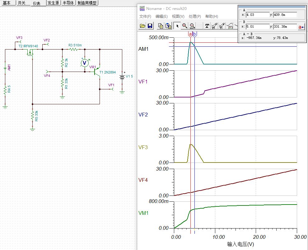
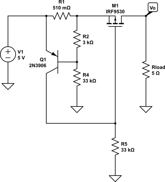
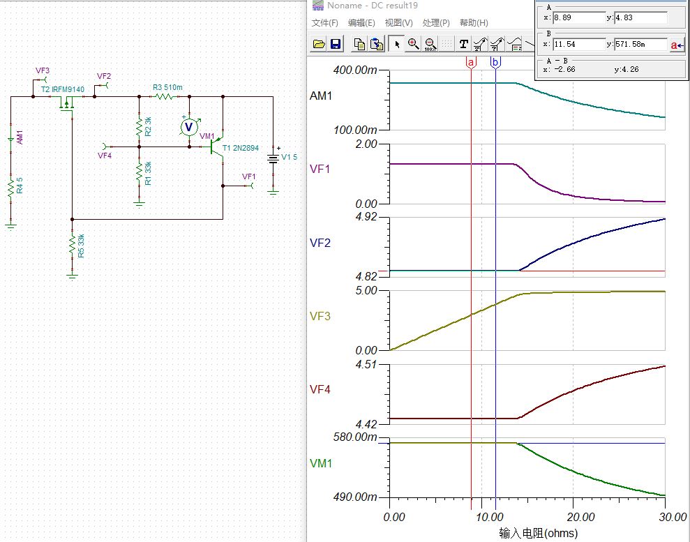 This is a current limit, can anybody give me some instructions about how to calculate the limited current?